
Huishi Tang, Zhili Chen, Li Tang, Yingxue Hui, Weiguo Liu. Preparation and Analysis of Lithium Niobate Nanostructures[J]. Chinese Journal of Lasers, 2023, 50(1): 0113018
- Chinese Journal of Lasers
- Vol. 50, Issue 1, 0113018 (2023)
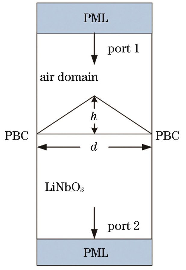
Fig. 1. Diagram of subwavelength structure simulation model
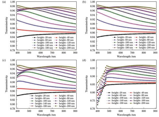
Fig. 2. Variations of level 0 transmissivity with structure height under different periods. (a) Period of 50 nm; (b) period of 100 nm;
Fig. 3. AFM images of LiNbO3 sample surface after etching with different incident energies, where the lower left corner is Fourier transform (FFT) image and the arrow indicates ion beam incidence direction (incident angle is 70°, etching time is 60 min and ion beam current is 40 mA). (a) Incident energy is 400 eV; (b) incident energy is 600 eV; (c) incident energy is 800 eV; (d) incident energy is 1000 eV
Fig. 4. PSD curves, height and RMS roughness of nanostructure on LiNbO3 sample surface after etching with different incident energies (incident angle is 70°, etching time is 60 min and ion beam current is 40 mA). (a) PSD curves; (b) height and RMS roughness of nanostructure
Fig. 5. AFM images of LiNbO3 sample surface after etching with different ion beam currents, where the lower left corner is FFT image and the arrow indicates ion beam incidence direction (incident angle is 70°, etching time is 60 min and incident energy is 1000 eV). (a) Ion beam current is 20 mA; (b) ion beam current is 30 mA; (c) ion beam current is 40 mA; (d) ion beam current is 50 mA
Fig. 6. PSD curves, height and RMS roughness of nanostructure on LiNbO3 sample surface after etching with different ion beam current (incident angle is 70°, etching time is 60 min and incident energy is 1000 eV). (a) PSD curves; (b) height and RMS roughness of nanostructure
Fig. 7. AFM images of LiNbO3 sample surface after different etching time, where the lower left corner is FFT image and the arrow indicates ion beam incidence direction (incident angle is 70°, ion beam current is 40 mA and incident energy is 1000 eV). (a) Etching time is 20 min; (b) etching time is 40 min; (c) etching time is 60 min; (d) etching time is 80 min; (e) etching time is 100 min; (f) etching time is 120 min
Fig. 8. PSD curves, height and RMS roughness of nanostructure on LiNbO3 sample surface after etching with different time (incident angle is 70°, ion beam current is 40 mA and incident energy is 1000 eV). (a) PSD curves; (b) height and RMS roughness of nanostructure
Fig. 9. Transmissivity curves of LiNbO3 sample surface and height and RMS roughness of conical nanostructure. (a)-(c) Transmissivity curves of LiNbO3 sample surface after etching with different ion beam parameters at 70° incident angle; (d)-(f) height and RMS roughness of conical structure
Fig. 10. Transmissivity of LiNbO3 surface ( incident angle is 70°, incident energy is 1000 eV and ion beam current is 40 mA).
Fig. 11. Comparison between simulated and measured transmissivity of LiNbO3 samples under different etching time (incident angle is 70°, ion beam current is 40 mA and incident energy is 1000 eV)


Set citation alerts for the article
Please enter your email address

© Copyright 2018-2021 | Chinese Laser Press. All Rights Reserved 沪ICP备15018463号-20