
Shan Gao, Chong-Yang Zhang, Hong-Rui Ao, Hong-Yuan Jiang. Performance of beam-type piezoelectric vibration energy harvester based on ZnO film fabrication and improved energy harvesting circuit[J]. Chinese Physics B, 2020, 29(8):
- Chinese Physics B
- Vol. 29, Issue 8, (2020)
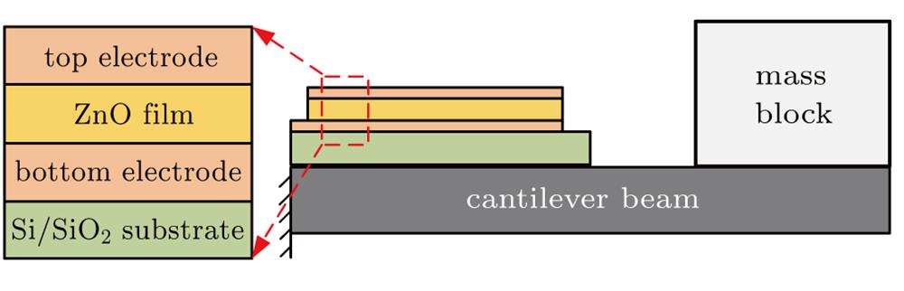
Fig. 1. Schematic diagram of piezoelectric energy harvesting vibrator.
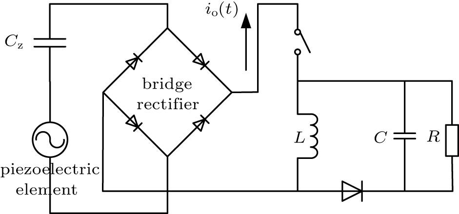
Fig. 2. Schematic diagram of SECE circuit.
Fig. 3. Schematic diagram of thyristor switch.
Fig. 4. Schematic diagram of ISECE circuit.
Fig. 5. Schematic diagram of spring–damping–mass vibration model.
Fig. 6. Surface topography of sputtered ZnO film under magnification factor of 8000.
Fig. 7. XRD spectrum of sputtered ZnO film.
Fig. 8. Schematic diagram of experimental setup.
Fig. 9. Experimental apparatus of whole energy harvester testing system.
Fig. 10. Plots of theoretical voltage output U versus frequency f for four different thickness values of ZnO film.
Fig. 11. Plots of theoretical voltage output U versus frequency f of ZnO film under four different external forces.
Fig. 12. Plots of theoretical output power P versus resistance in SECE and ISECE circuits.
Fig. 13. Plots of experimental voltage output U versus frequency f under three different forces.
Fig. 14. Experimental output power P versus resistance R in SECE and ISECE circuits.
|
Table 1. Dimensions of piezoelectric components in vibrator.
|
Table 2. Specifications of components in ISECE circuit.
|
Table 3. Deposition parameters of ZnO film.
|
Table 4. Surface topography testing values of ZnO film.

Set citation alerts for the article
Please enter your email address
© Copyright 2018-2021 | Chinese Laser Press. All Rights Reserved 沪ICP备15018463号-20