
Hui Long, Jian-Wei Hu, Fu-Gen Wu, Hua-Feng Dong. Ultrafast pulse lasers based on two-dimensional nanomaterial heterostructures as saturable absorber [J]. Acta Physica Sinica, 2020, 69(18): 188102-1
- Acta Physica Sinica
- Vol. 69, Issue 18, 188102-1 (2020)
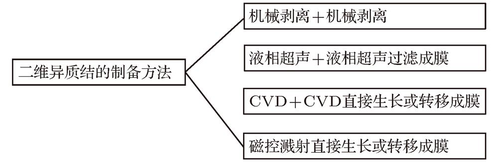
Fig. 1. Fabrication methods of two-dimensional heterostructure saturable absorbers.
![(a) Schematic of α-MoTe2/MoS2 heterostructure prepared by mechanical exfoliation[40]; (b) the optical microscopy image[40].](/richHtml/wlxb/2020/69/18/20201235/img_2.jpg)
Fig. 2. (a) Schematic of α-MoTe2/MoS2 heterostructure prepared by mechanical exfoliation[40]; (b) the optical microscopy image[40].
Fig. 3. (a) Illustration of preparation procedures of WS2/Graphene heterostructure films by liquid phase exfoliation, a series of of WS2/Graphene heterostructure films with different thickness obtained from different filtration volume; (b) atomic force microscopy image of WS2/Graphene heterostructure films; (c) X-ray diffraction patterns; (d) absorption as a function of filtration volume at 800 nm; (e) open-aperture Z-scan results of WS2, Graphene, and WS2/Graphene heterostructure films with the thickness of ~135 nm; (f) histogram of the imaginary part of the third-order nonlinear coefficient Imχ (3) and figure of merit (FOM) of WS2, Graphene, and WS2/Graphene heterostructure[41].
Fig. 4. (a) Illustration of preparation procedures of MoTe2/MoS2 heterostructure films by liquid phase exfoliation; (b) Z-scan results of MoTe2, MoS2 and MoTe2/MoS2 heterostructure films under the pump intensity of 606 GW·cm–2 with the thickness of ~80 nm; (c) Z-scan results of MoTe2/MoS2 heterostructure films with thickness of 30, 60, 80, 100, 120 nm at 606 GW·cm–2, respectively[47].
Fig. 5. (a) Schematic and (b) Raman spectrum of MoS2/WS2 heterostructure[53]; (c) optical microscope photograph of monolayer triangular WS2 grown on monolayer MoS2 nanosheet; (d) photoluminescence (PL) spectrum of WS2 monolayer, MoS2 monolayer and MoS2/WS2 heterostructure[54]; (e) schematic diagram of as-grown Bi2Te3/Graphene heterostructure on SiO2/Si substrate; (f) absorption spectrum of Graphene and Bi2Te3/Graphene heterostructure[55].
Fig. 6. (a) AFM image of Bi2Te3/Graphene heterostructure fabricated by two-step CVD method on the SiO2 substrate; (b) thickness profiles along line 1 in (a); (c) absorption spectrum of Bi2Te3/Graphene heterostructure from 900−2000 nm[56]; (d) schematic of WS2/ Graphene heterostructure after transferring successfully; (e) Z-scan graph of WS2, Graphene and WS2/Graphene heterostructure[32]
Fig. 7. Scanning electron microscope images of MoS2/WS2 heterostructure from the top view (a) and side view (b); (c) Raman spectrum of MoS2, WS2 and MoS2/WS2 heterostructure; (d) transmission of MoS2/WS2 heterostructure with respect to the power intensity of incident light[57].
Fig. 8. (a) Illustration of band alignment and carrier mobility of the type-II MoS2/WS2 heterostructure[63]; (b) band alignment of semiconductor type-II MoTe2/MoS2 heterostructure[47]; (c) diagram of the charge-transfer process in a MoS2/graphene heterostructure[64]; (d) energy band diagram of Bi2Te3/graphene heterojunction, the blue dots stand for the photogenerated electrons, while red hollow dots stand for holes[55].
Fig. 9. Recorded results of Te/BP heterojunction SAM-based mode-locked laser: (a), (b) measured autocorrelation trace of 404 fs and the corresponding spectrum; (c), (d) recorded frequency spectrum with a wide and a narrow span respectively[65]; (e) schematic setup of the Q -switched mode-locking (QML) laser and (f) the output power versus pump power of the continuous wave (CW) and QML operation for MoS2/Graphene heterostructure[34]
Fig. 10. (a) Schematic of graphene/MoS2 heterojunction mode-locked laser device; (b) pulse trains; (c) spectrum; (d) autocorrelation race for 92 fs duration; (e) frequency spectrum[66].
Fig. 11. (a)−(c) Mode-locking performance of Graphene/WS2 heterostructure: (a) Optical spectrum; (b) pulse trains; (c) autocorrelation trace[69]. (d)−(f) Mode-locking performance of Graphene/Mo2C heterostructure: (d) Optical spectrum; (e) pulse trains; (f) autocorrelation trace[70]. (g)−(i) Mode-locking performance of Graphene/phosphorene heterostructure: (g) Optical spectrum; (h) pulse trains; (i) autocorrelation trace[71].
Fig. 12. (a) Schematic of Graphene/Bi2Te3 heterostructure on the end-facet of fiber connector; (b)−(d) Mode-locking characteristics of Graphene/Bi2Te3 heterostructure: (b) Optical spectrum; (c) pulse trains; (d) autocorrelation trace[72]. (e) Schematic of Er-doped fiber laser. (f)−(h) Mode-locking characteristics of Bi2Te3/FeTe2 heterostructure: (f) Optical spectrum; (g) pulse trains; (h) autocorrelation trace[73]. (i) Schematic of Er-doped fiber laser. (j)−(l) Mode-locking characteristics of Graphene/MoS2 heterostructure: (j) Optical spectrum; (k) pulse trains; (l) autocorrelation trace[74].
Fig. 13. (a) Experimental setup of mode-locked fiber laser with 1550 nm QD-SESAM; Inset: cross-sectional transmission electron microscope image of the QD-SESAM and 1 μm × 1 μm AFM image of the 1550 nm QDs. (b)−(e) Characteristics of mode-locked the developed fiber laser of InAs/GaAs QD: (b) Output power versus pump power; (c) output optical spectra; (d) RF spectrum of the mode-locked fiber laser; (e) autocorrelation trace[75].
Fig. 14. (a) Schematic of deposition of the Te/Se sample on the microfiber. (b)−(d) Mode locking performance of the Te-based fiber laser: (b) Optical spectrum; (c) pulse trains; (d) autocorrelation trace. (e) Te/Se samples under microscope with 50 μm scale. (f)−(h) Self-starting mode locking performance of the Yb-doped fiber laser: (f) Optical spectrum; (g) pulse trains; (h) autocorrelation trace[76].
Fig. 15. (a)−(c) Mode-locking performance of MoS2/WS2 heterostructure: (a) Optical spectrum; (b) pulse trains; (c) autocorrelation trace[57]. (d)−(f) Mode-locking performance of MoS2/Sb2Te3/MoS2 heterostructure: (d) Optical spectrum; (e) pulse trains; (f) autocorrelation trace[77]. (g)−(i) Mode-locking performance of WS2/MoS2/WS2 heterostructure: (g) Optical spectrum; (h) RF spectrum; (i) autocorrelation trace[63].
| ||||||||||||||||||||||||||||||||||||||||||||||||||||||||||||||||||||||||||||||||||||||||||||||||||||||||||||||||||||||||||||||||||||||||||||||||||||||||||||||||||||||||||||||||||||||||||||||||||||||||||||
Table 1. [in Chinese]


Set citation alerts for the article
Please enter your email address

© Copyright 2018-2021 | Chinese Laser Press. All Rights Reserved 沪ICP备15018463号-20