Abstract
An ultra-compact hybrid-integration receiver optical subassembly (ROSA) with four channels is demonstrated in our laboratory with the size of 23.3 mm × 6.0 mm × 6.5 mm. The ROSA is comprised of a planar lightwave circuit (PLC) arrayed waveguide grating (AWG) chip, a top-illuminated positive-intrinsic-negative photodetector array chip, and a three-dimensional microwave circuit that is specially designed for compact packaging. For each transmission lane, the 3 dB bandwidth of the ROSA is up to 20 GHz, and the maximum responsivity is up to 0.53 A/W. The proposed package structure can be used for smaller package sizes and would be an easy assembling solution for 100 GbE optical communication devices.With the rapid growth of data traffic for hyper-scale internet data centers, the demand for high speed optical transceiver modules to interconnect among the intra and inter data centers beyond 100 Gbit/s becomes strong. To meet the demand, 100 Gigabit Ethernet (GbE) was standardized in 2010, and 400 GbE is now being standardized by an Institute of Electrical and Electronics Engineers (IEEE) task force[1]. The 100 GbE standard defines four transmission channels using wavelength division multiplexing (WDM) technology to achieve high capacity transmission. Coarse wavelength division multiplexer (CWDM) and local area network (LAN) WDM are two commonly used wavelength allocations that comply with the International Telecommunication Union (ITU) standards. For CWDM, the center wavelengths of the four channels are 1270 nm (Lane 0), 1290 nm (Lane 1), 1310 nm (Lane 2), and 1330 nm (Lane 3), and the center wavelengths of the four channels for LAN-WDM are 1295.56 nm (lane 0), 1300.05 nm (lane 1), 1304.58 nm (lane 2), and 1309.14 nm (lane 3), respectively[2]. Due to the wide wavelength spacing of the CWDM system, it reduces the requirements for lasers. For example, the emission wavelength accuracy of the laser can be relaxed to . Moreover, within the operating temperature range of , the wavelength drift caused by temperature changes is still within the allowable range. Therefore, the lasers in the CWDM system do not require chillers to keep the temperature constant, resulting in reducing power consumption of the system. In addition, the larger wavelength interval means that the structure of the optical multiplexer (MUX)/demultiplexer (DEMUX) is greatly simplified, which leads to an increase in yield and a cost reduction.
Due to the limited space of the high port density line card data network center, the optical transceivers modules with small form factor and low power consumption are required to increase port density of line cards in communication systems. One of the key issues for miniaturization is hybrid integration technology to assemble various discrete components in an ultra-compact tube, such as integration of laser chips, microwave circuit, optical MUX, and focusing lenses into a transmitter optical subassembly (TOSA) module[3,4] or integration of a photodetector (PD) array chip and optical DEMUX into a receiver optical subassembly (ROSA) module[5,6]. In order to achieve a compact package and enhance the performances of the packaged module at the same time, researchers have done a mountain of studies. For example, in 2011, Nippon Telegraph and Telephone (NTT) Photonics Laboratories reported a compact TOSA with the size of . To decrease the electrical crosstalk and realize smaller volume, a novel bridge-type radio frequency (RF) circuit board was proposed[7]. Then, in 2013, their group developed the first ultra-compact 100 GbE TOSA, a very small volume of , in which a three-dimensional (3D) RF circuit board supported by a spacer was designed[8,9]. In Ref. [10], a 3D RF impedance matching circuit was demonstrated for the packaging of an electroabsorption modulation laser (EML) array. However, most of these studies are about TOSA modules. In the packaging process of ROSA modules, the microwave circuit usually contains two parts of an RF circuit and a bias network on which many capacitors and resistors are mounted. If they are all installed in the one circuit board, it will easily cause crosstalk and distortion of the electrical signals. To overcome this drawback, in this paper, a 3D microwave circuit that allows the RF signal and bias voltage to be isolated in physical space is proposed for compact packaging. In the packaging progress, a silicon-based 40° planar lightwave circuit (PLC) arrayed waveguide grating (AWG) chip, high frequency electrical traces, DC bias circuit board, and a top-illuminated PIN PD array chip are hybridly integrated in a compact tube. With the optimized scheme, the bandwidths of the four RF lines all reach 60 GHz, and the reflection is less than in the range of 0 to 60 GHz. Moreover, the electrical crosstalk between the adjacent lanes is below . The bandwidths of four channels of the fabricated module are all up to 20 GHz assigned in 100 GbE. The maximum responsivity is 0.53 A/W. In this Letter, the detailed design of the proposed ROSA structure, the simulation of RF circuit board, the equivalent circuit model of the PD module, and the test results of the fabricated ROSA are presented and discussed.
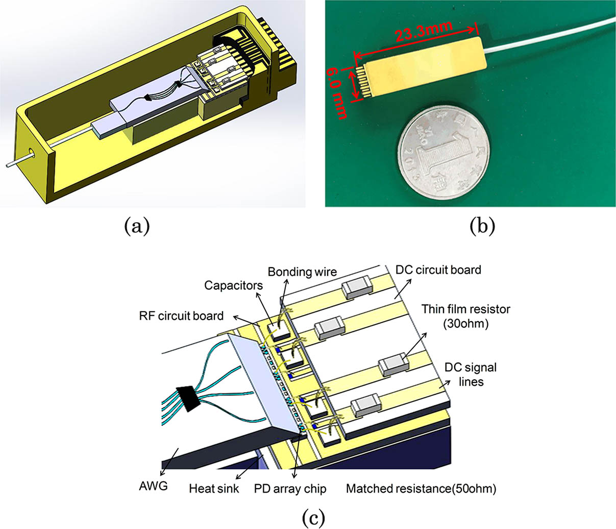
Figure 1(a) shows the cross-sectional view of the proposed ROSA module configuration. It consists of an ultra-compact package shell, a four-channel top-illuminated PIN PD array chip, a 3D microwave circuit on which bypass capacitors and partial resistances are bonded, and a silica-based CWDM operated at the O band with 20 nm wavelength spacing. The transmitted optical signals are divided into four lanes with independent wavelengths by the AWG, and then four independent signals are converted into electrical signals by the PD array chip. The photograph of the ROSA, whose size is , is shown in Fig. 1(b), and the partially detailed configuration is shown in Fig. 1(c). It can be seen that microwave circuit is designed into two layers. The DC lines and signal lines are placed on different inner circuit boards that are stacked in the package. The PD array chip is mounted on the middle of AlN substrate by conductive plastic. To realize direct optical coupling between the output waveguides and the photosensitive surface of PDs, the end facet of the output waveguides of the AWG was polished to form a 40° reflection mirror. Compared to optical coupling in an optical prism or vertically mounted PDs, it greatly simplified the packaging process and reduced the manufacture cost.
Sign up for Chinese Optics Letters TOC. Get the latest issue of Chinese Optics Letters delivered right to you!Sign up now

Figure 1.(a) Hybridly-integrated CWDM ROSA module configuration. (b) Photograph of the ROSA. (c) Partially detailed configuration of the ROSA.
For the microwave circuit design, it is common to increase space between individual signal lines for reducing crosstalk between adjacent channels. However, if four RF lines and four bias circuit networks are all installed inside a planar circuit board in the ultra-compact packaging of ROSA, the electrical crosstalk will be increased due to the small pitch of the RF signal lines and intricate power cord. To solve this problem, a simple and effective scheme with a 3D microwave circuit has been proposed, as shown in Fig. 2. The signal lines and bias circuit networks are placed on two different circuit boards, and then they are stacked vertically with spacers at a pitch of 0.5 mm. The bias circuit networks are fabricated on the top layer, on which the thin film resistors are installed to adjust the static working bias point of the PDs. The RF circuit board, including bypass capacitors, a four-lane PIN PD array chip, and four termination resistances, is assembled on the bottom layer.
Figure 2.(a) Schematic of 3D microwave circuit. (b) Model of RF circuit board with high frequency transmission line.
The internal resistance of the PD during operation is very large, which is up to the mega ohm level, thus 50 ohm matching resistors are used and placed in parallel with the chip in order to match with the 50 ohm measurement system. The terminating resistors here are directly fabricated on the AlN substrate in the form of thin film resistors, which are placed between the signal line and the ground to achieve parallel connection with the PDs and realize independence matching. The electrodes and electrodes of the PD chips are connected to the upper surfaces of chip capacitors and signal line by wire bonding, respectively, and the upper surfaces of chip capacitors on the bottom circuit board are also connected to the DC lines through bonding wires to provide bias voltages for the detector chip. To optimize the high frequency performance of the module, the chip capacitor should be as close as possible to the PD array chip within the allowable range of space.
Figure 2(b) shows the model of RF circuit board with a high frequency transmission line, whose structure is a grounded coplanar waveguide (GCPW). The RF circuit board is made of AlN ceramic. The designed size of the AlN substrate is . The ratio of the width of the signal lines and the gap between the signal lines determines the characteristic impedance of the transmission lines. In order to reduce electrical reflections, the characteristic impedance of the GCPW transmission lines should be designed to be 50 ohm. After calculation, the width of the signal lines and the gap between the signal lines are designed to be 0.12 and 0.08 mm, respectively. The length of the signal lines is 2.8 mm. Generally, via holes are often adopted to get a good ground connection. However, the size and position of the via holes need to be carefully designed; otherwise, it will bring resonance and other effects, which will seriously affect the transmission performance. To simplify the production process and reduce fabrication costs, connecting all ground lines together is a simple and effective solution, as shown in Fig. 2(b).
Figure 3 shows the simulation results of transmission performance of the RF circuit board, which is a typical simulation result of insertion loss (S21) and return loss (S22). The result shows that the bandwidths of the designed transmission lines all reach 60 GHz, and the reflection is less than in the range of 0–60 GHz, which far from meet the design requirements of the module for 20 GHz. Figure 4 shows the simulation results of the electrical crosstalk between the adjacent channels. It indicated that the electrical crosstalk between the adjacent lane 12 and lane 23 is below in the frequency range of 0 to 60 GHz, which can be ignored. With the proposed scheme, the crosstalk between signal lines can be well suppressed.
Figure 3.Simulation results of transmission performance of the RF circuit board.
Figure 4.Simulation results of the electrical crosstalk between the adjacent channels.
To evaluate the impact of each part of the packaging process, a small-signal equivalent circuit model for one channel is established in Advanced Design System (ADS). The detailed circuit model is presented in Fig. 5. The intrinsic circuit model for the PD chip is marked by a red dot line. The carrier transit time effect of the PD is characterized by the approximate Rt·Ct time constant. The photo-generated current of the PD is controlled by a voltage controlled current source (VCCS) model[11], in which the parameter G0 is a representation of quantum efficiency for the PD chip. Rj and Cj are modeled as the junction resistance and capacitance of the active region, respectively. Ca represents the capacitance between the contact electrodes, Rb is associated with the non-depletion layer resistance. The equivalent circuit except the red dot line area represents the parasitic network introduced by package progress. The parameters Ls, Rs, and Cs are introduced by wire bonding. Particularly, Ls and Rs are associated with the parasitic inductance and resistance. Cs represents the parasitic capacitance between the chip and substrate. The RF circuit board is characterized by a coplanar waveguide (CPW) model, whose parameters are consistent with the actual board size. Rs1 and Ls1 represent the parasitic parameters introduced by the feed-wall structure. The parasitic capacitance that was introduced by the solder used in the package is characterized by C2.
Figure 5.Small-signal equivalent circuit model for one channel of the module.
The values of the individual components can be tuned to observe changes of the frequency response curve to evaluate the impact of each part of the package progress. Here, the parasitic inductance introduced by wire bonding and parasitic inductance introduced by solder are mainly investigated. Figure 6 shows the calculated frequency response with different values of Ls. The result indicates that the −3 dB bandwidth of the module will increase significantly with the increase of inductance, which ranges from 0 to 0.3 nH. However, when the inductance increases to 0.4 nH, the bandwidth is reduced, but the flatness of the frequency response curve is improved. Therefore, the inductance can be used to extend the bandwidth of the PD in case of controlling the length of the gold wire within a certain range. In addition, the parasitic capacitance introduced by the solder is also studied seriously. As shown in Fig. 7, the gain of the PD is reduced slightly when the capacitance increases from 0 to 100 fF with steps of 50 fF. When the capacitance continues to increase from 100 fF, the bandwidth drops by 1 GHz for every 50 fF increase in capacitance. So, the parasitic effects introduced by solder should be minimized as much as possible. Figure 8 shows the measured and simulation frequency response of the PD chip and the packaged module for one channel. The inset figures are their corresponding simulation eye diagrams.
Figure 6.Calculated frequency response with different values of Ls.
Figure 7.Calculated frequency response with different values of C2.
Figure 8.Measured and simulation frequency responses of (a) the PD chip and (b) the packaged module for one channel. The insets are their corresponding simulation and measurement eye diagrams.
With the help of the parasitic parameter compensation technique in the proposed scheme, the bandwidth of the packaged module is larger than that of the PD chip. As exhibited in Fig. 8, the bandwidths of the PD array chip and packaged PD module are about 18 and 20 GHz, respectively. With the optimized scheme, the bandwidth optimization could up to 2–3 GHz. As shown in Fig. 8, the simulation and test eye diagrams of the packaged module are clearer than those of the PD chip.
In the ROSA module, the commercially available top-illuminated PIN PD array chip with a pitch of 750 μm is employed, whose photosensitive surface diameter is 20 μm, and responsivity is up to 0.8 A/W. Because the direction of light transmission in the AWG waveguide is horizontal and the PD array’s illumination area is on the top, it is necessary to change the optical axis or the electric axis to realize optical coupling. Generally, a vertically mounted PD chip with 90° gold wire or gold belt bonding could change the electric axis, but the fabrication process is complex, and the high frequency performance of the device would be seriously affected. Here, an AWG with a 40° output end facet is adopted to change the four-optical-beam axis to the package bottom; it significantly simplified the packaging process. The packaged ROSA module possesses a broad flat-top spectral profile, as shown in Fig. 9, in which the gray area represents the wavelength range in the IEEE 802.3ba standard. The flat-top profile provided a much wider tolerance to wavelength drift caused by temperature changes. Figure 10 shows the measured response curves of the packaged ROSA module, and the photograph of the module with the detailed inner distribution is inserted. As shown in Fig. 10, first, the PD array chip is mounted on an AlN carrier by silver epoxy, and then their electrodes are led out by gold wire bonding, preparing for active optical coupling. The AWG chip is held by a fixture, and then moved parallel to the PD array chip. Based on the PD generated output photocurrent, when it reaches the maximum, the AWG chip would be fixed with UV-curable adhesive. It shows that the responsivities of lanes 0, 1, 2, and 3 are 0.45, 0.52, 0.53, and 0.48 A/W, respectively. The result indicates that the saturated input optical powers of four lanes all reach 9 mW, which are enough for the non-return to zero (NRZ) modulation format.
Figure 9.Flat-top spectral profile of four-lane ROSA module in CWDM (gray areas indicate CWDM grid).
Figure 10.Measured responsivity of the packaged ROSA module. Inset is the photograph of the module with the detailed inner distribution.
Figure 11 shows the measured transmission response and reflection response of the hybridly-integrated PD module at a bias voltage of 3 V. It indicates that the bandwidths for all channels are up to 20 GHz, and the reflection coefficients for four lanes are less than in the range of 0 to 20 GHz. The module can be used to achieve 100 Gb/s total capacity data transmission.
Figure 11.Measured transmission response and reflection response of the hybridly-integrated PD module at a bias voltage of 3 V.
In conclusion, an ultra-compact ROSA with a 3D microwave circuit is fabricated in our laboratory. The bandwidth of each lane is up to 20 GHz. To evaluate the impact of parasitic parameters, a small-signal equivalent circuit model for one lane is established. The frequency response results are in very good agreement between the modeling and the experimental measurements. The module is used not only for NRZ modulation transmission, but also for many RF transmission systems, such as remote antennas, satellite antennas, and secure encrypted communication. In addition, it can also be applied to radar systems to achieve full-band detection of radar.
References
[1]
[2] J. K. Lee, S.-K. Kang, J. Y. Huh, Y.-S. Jang. European Conference and Exhibition on Optical Communication, 888(2013).
[3] Z. Zhang, Y. Liu, J. An, Y. Zhang, Z. Zhao, J. Liu, N. Zhu. Chin. Opt. Lett., 16, 062501(2018).
[4] S. Kanazawa, T. Fujisawa, N. Nunoya, A. Ohki, K. Takahata, H. Sanjoh, R. Iga, H. Ishii. J. Lightwave Technol., 31, 602(2013).
[5] Y. Doi, M. Oguma, M. Ito, I. Ogawa, T. Yoshimatsu, T. Ohno, E. Yoshida, H. Takahashi. National Fiber Optic Engineers Conference, NW1J.5(2013).
[6] K. Park, G. D. Lee, S. N. Lee, H.-G. Park, W.-Y. Hwang, J. Choi, K.-H. Yang. 2017 European Conference on Optical Communication (ECOC)(2017).
[7] S. Kanazawa, T. Fujisawa, A. Ohki, H. Ishii, N. Nunoya, Y. Kawaguchi, N. Fujiwara, K. Takahata, R. Iga, F. Kano, H. Oohashi. IEEE J. Sel. Top. Quantum Electron., 17, 1191(2011).
[8] T. Fujisawa, T. Itoh, S. Kanazawa, K. Takahata, Y. Ueda, R. Iga, H. Sanjo, T. Yamanaka, M. Kotoku, H. Ishii. Opt. Express, 21, 182(2013).
[9] S. Kanazawa, T. Fujisawa, N. Nunoya, A. Ohki, K. Takahata, H. Sanjoh, R. Iga, H. Ishii. J. Lightwave Technol., 31, 602(2013).
[10] Z. Zhang, Y. Liu, J. Wang, J. Bai, H. Yuan, X. Wang, J. Liu, N. Zhu. IEEE Photon. J., 8, 2700912(2016).
[11] G. Wang, T. Tokumitsu, I. Hanawa, K. Sato, M. Kobayashi. IEEE Microwave Wireless Compon. Lett., 12, 378(2002).