• Acta Physica Sinica
  • Vol. 69, Issue 18, 187701-1 (2020)
Ju-Shan Wang1, Jin-Peng Ma1, Xiang-Yong Zhao1、*, Ming-Zhu Chen1, Fei-Fei Wang1, Tao Wang1, Yan-Xue Tang1, Wei Cheng1、*, Di Lin2, and Hao-Su Luo2
Author Affiliations
  • 1Mathematics and Science College, Shanghai Normal University, Shanghai 200234, China
  • 2Artificial Crystal Research Center, Shanghai Institute of Ceramics, Chinese Academy of Sciences, Shanghai 201899, China
  • show less
    DOI: 10.7498/aps.69.20200544 Cite this Article
    Ju-Shan Wang, Jin-Peng Ma, Xiang-Yong Zhao, Ming-Zhu Chen, Fei-Fei Wang, Tao Wang, Yan-Xue Tang, Wei Cheng, Di Lin, Hao-Su Luo. Preparation and ferroelectric domain structure of micro-scale piezoelectric array fabricated by Mn doped Pb(In1/2Nb1/2)O3-Pb(Mg1/3Nb2/3)O3-PbTiO3single crystal [J]. Acta Physica Sinica, 2020, 69(18): 187701-1 Copy Citation Text show less
    Flow chart of the whole experiment.
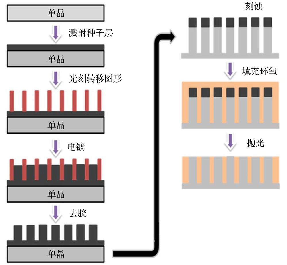
    Fig. 1. Flow chart of the whole experiment.
    Results of lithography: (a), (b) Surface morphology under optical microscope and cross section under scanning electron microscope when the element size is 12.94 μm; (c), (d) surface morphology under optical microscope and cross section under scanning electron microscope when the element size is 13.97 μm.
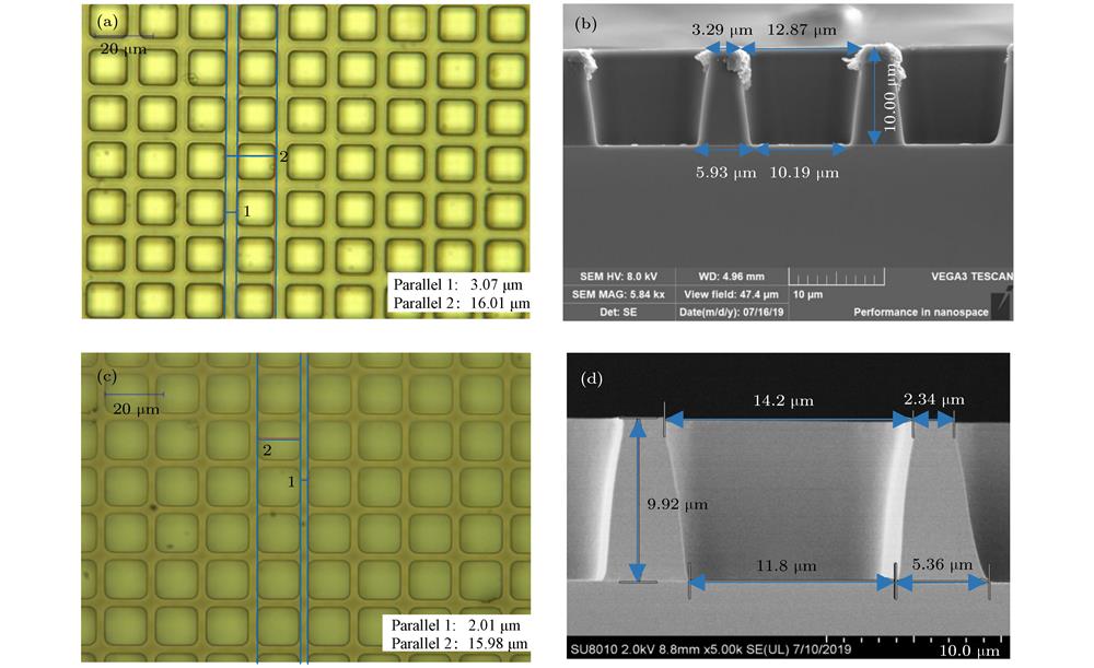
    Fig. 2. Results of lithography: (a), (b) Surface morphology under optical microscope and cross section under scanning electron microscope when the element size is 12.94 μm; (c), (d) surface morphology under optical microscope and cross section under scanning electron microscope when the element size is 13.97 μm.
    Schematic diagram of lithographic pattern structure.
    Fig. 3. Schematic diagram of lithographic pattern structure.
    Electroplating experiment results: (a) Surface under scanning electron microscope; (b) cross section under scanning electron microscope.
    Fig. 4. Electroplating experiment results: (a) Surface under scanning electron microscope; (b) cross section under scanning electron microscope.
    Etching rate experimental results: (a) Relationship between etching rate and antenna power; (b) relationship between etching rate and bias power; (c) relationship between etching rate and etching gas flow ratio.
    Fig. 5. Etching rate experimental results: (a) Relationship between etching rate and antenna power; (b) relationship between etching rate and bias power; (c) relationship between etching rate and etching gas flow ratio.
    Etching results: (a) Surface morphology of high density array; (b) cross section morphology of high density array; (c) cross section morphology of conical array; (d) the surface morphology of deep etching of high density surface array.
    Fig. 6. Etching results: (a) Surface morphology of high density array; (b) cross section morphology of high density array; (c) cross section morphology of conical array; (d) the surface morphology of deep etching of high density surface array.
    Structure of different scale areas under the piezoelectric microscope: (a) Surface morphology of 30 μm × 30 μm area; (b) out of plane amplitude of 30 μm × 30 μm area; (c) phase of 30 μm × 30 μm area; (d) surface morphology of 5 μm × 5 μm area; (e) out of plane amplitude of 5 μm × 5 μm area; (f) phase of 5 μm × 5 μm area; (g) surface morphology of 1 μm × 1 μm area; (h) out of plane amplitude of 1 μm × 1 μm area; (i) phase of 1 μm × 1 μm area.
    Fig. 7. Structure of different scale areas under the piezoelectric microscope: (a) Surface morphology of 30 μm × 30 μm area; (b) out of plane amplitude of 30 μm × 30 μm area; (c) phase of 30 μm × 30 μm area; (d) surface morphology of 5 μm × 5 μm area; (e) out of plane amplitude of 5 μm × 5 μm area; (f) phase of 5 μm × 5 μm area; (g) surface morphology of 1 μm × 1 μm area; (h) out of plane amplitude of 1 μm × 1 μm area; (i) phase of 1 μm × 1 μm area.
    Results of 1 μm × 1 μm area under the piezoelectric force microscope: (a) Out of plane amplitude at ± 10 V; (b) phase at ± 10 V; (c) out of plane amplitude at ± 20 V; (d) phase at ± 20 V; (e) out of plane amplitude at ± 30 V; (f) phase at ± 30 V.
    Fig. 8. Results of 1 μm × 1 μm area under the piezoelectric force microscope: (a) Out of plane amplitude at ± 10 V; (b) phase at ± 10 V; (c) out of plane amplitude at ± 20 V; (d) phase at ± 20 V; (e) out of plane amplitude at ± 30 V; (f) phase at ± 30 V.
    Electric field induced amplitude and phase evolution in situ in the 1 μm × 1 μm area at room temperature
    Fig. 9. Electric field induced amplitude and phase evolution in situ in the 1 μm × 1 μm area at room temperature
    成分含量
    氨基磺酸镍/g·L–1280—400
    硼酸/g·L–140—50
    阳极活化剂/g·L–160—100
    润湿剂/mL·L–11—5
    去应力剂适量
    Table 1.

    Composition and content of electroplate bath ingredients.

    电镀液配料成分及含量

    Ju-Shan Wang, Jin-Peng Ma, Xiang-Yong Zhao, Ming-Zhu Chen, Fei-Fei Wang, Tao Wang, Yan-Xue Tang, Wei Cheng, Di Lin, Hao-Su Luo. Preparation and ferroelectric domain structure of micro-scale piezoelectric array fabricated by Mn doped Pb(In1/2Nb1/2)O3-Pb(Mg1/3Nb2/3)O3-PbTiO3single crystal [J]. Acta Physica Sinica, 2020, 69(18): 187701-1
    Download Citation