• Photonics Research
  • Vol. 11, Issue 6, 1057 (2023)
Yunqing Jiang1、2、†, Hongqing Li2、3、†, Xiaoqiang Zhang1、2、*, Fan Zhang1、2, Yong Xu1、2, Yongguang Xiao3, Fengguang Liu1、2, Anting Wang4, Qiwen Zhan5, and Weisheng Zhao1、2
Author Affiliations
  • 1School of Integrated Circuit Science and Engineering, Hefei Innovation Research Insititute, Beihang University, Beijing 100191, China
  • 2Anhui High Reliability Chips Engineering Laboratory, Hefei 230013, China
  • 3School of Materials Science and Engineering, Xiangtan University, Xiangtan 411105, China
  • 4Department of Optics and Optical Engineering, University of Science and Technology of China, Hefei 230026, China
  • 5School of Optical-Electrical and Computer Engineering, University of Shanghai for Science and Technology, Shanghai 200093, China
  • show less
    DOI: 10.1364/PRJ.487711 Cite this Article Set citation alerts
    Yunqing Jiang, Hongqing Li, Xiaoqiang Zhang, Fan Zhang, Yong Xu, Yongguang Xiao, Fengguang Liu, Anting Wang, Qiwen Zhan, Weisheng Zhao. Promoting spintronic terahertz radiation via Tamm plasmon coupling[J]. Photonics Research, 2023, 11(6): 1057 Copy Citation Text show less
    (a) Schematic illustration of the spin thin films without TPC and with TPC structure for THz radiation. (b) Phase of r1, r2, and r1r2 exp[i(4πnSiO2dinsert)/λ] as a function of wavelength, when the thickness of the optical cavity is 57 nm. (c) Simulated reflectance spectra of the dielectric layers as a function of incidence angle and wavelength for TM polarization.
    Fig. 1. (a) Schematic illustration of the spin thin films without TPC and with TPC structure for THz radiation. (b) Phase of r1, r2, and r1r2exp[i(4πnSiO2dinsert)/λ] as a function of wavelength, when the thickness of the optical cavity is 57 nm. (c) Simulated reflectance spectra of the dielectric layers as a function of incidence angle and wavelength for TM polarization.
    (a) Simulated absorptance varying with SiO2 cavity thickness dinsert and optical wavelength. (b) Absorptance spectra with different dinsert (dinsert=0 nm, 57 nm, 327 nm). (c)–(e) Normalized electric field profile distributions of point A (dinsert=0 nm, λ=743 nm), point B (dinsert=57 nm, λ=780 nm), and point C (dinsert=327 nm, λ=780 nm), respectively.
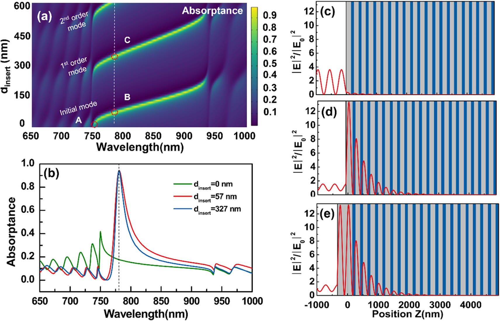
    Fig. 2. (a) Simulated absorptance varying with SiO2 cavity thickness dinsert and optical wavelength. (b) Absorptance spectra with different dinsert (dinsert=0  nm, 57 nm, 327 nm). (c)–(e) Normalized electric field profile distributions of point A (dinsert=0  nm, λ=743  nm), point B (dinsert=57  nm, λ=780  nm), and point C (dinsert=327  nm, λ=780  nm), respectively.
    (a) Cross-sectional SEM image of the spin thin films with a TPC structure. The average roughness of (b) spin thin films with TPC, (c) pure spin thin films, and (d) pure dielectric layers surface.
    Fig. 3. (a) Cross-sectional SEM image of the spin thin films with a TPC structure. The average roughness of (b) spin thin films with TPC, (c) pure spin thin films, and (d) pure dielectric layers surface.
    (a) Illustration of four comparison experiments of pure spin thin films without TPC, spin thin films with TPC, spin thin films with SiO2 substrate (without TPC+SiO2), spin thin films with pure dielectric layers (without TPC + dielectric layers). (b) THz waveforms and (c) the frequency-domain THz signals from the spin thin films without TPC (blue line, MAX is 406), the spin thin films with TPC (red line, MAX is 1072), without TPC+SiO2 (black line, MAX is 354), and without TPC + dielectric layers (green line, MAX is 356) at the pump fluence of 12.7 μJ/cm2. (d) Simulation absorptance spectra of the spin thin films with TPC and without TPC. (e) Maximum amplitude of generated THz electric field as a function of the pump laser power when its spot diameter is 1 cm.
    Fig. 4. (a) Illustration of four comparison experiments of pure spin thin films without TPC, spin thin films with TPC, spin thin films with SiO2 substrate (without TPC+SiO2), spin thin films with pure dielectric layers (without TPC + dielectric layers). (b) THz waveforms and (c) the frequency-domain THz signals from the spin thin films without TPC (blue line, MAX is 406), the spin thin films with TPC (red line, MAX is 1072), without TPC+SiO2 (black line, MAX is 354), and without TPC + dielectric layers (green line, MAX is 356) at the pump fluence of 12.7  μJ/cm2. (d) Simulation absorptance spectra of the spin thin films with TPC and without TPC. (e) Maximum amplitude of generated THz electric field as a function of the pump laser power when its spot diameter is 1 cm.
    Absorptance spectra of the spin thin film with TPC under different incident angles and wavelengths for (a) a TM pump beam and (b) a TE pump beam. (c) THz waveforms from the spin thin films with TPC under different polarization states at the pump fluence of 12.7 μJ/cm2. (d) Normalized maximum amplitude of THz waveforms from the spin thin films with TPC for a TM pump beam and a TE pump beam at different incident angles.
    Fig. 5. Absorptance spectra of the spin thin film with TPC under different incident angles and wavelengths for (a) a TM pump beam and (b) a TE pump beam. (c) THz waveforms from the spin thin films with TPC under different polarization states at the pump fluence of 12.7  μJ/cm2. (d) Normalized maximum amplitude of THz waveforms from the spin thin films with TPC for a TM pump beam and a TE pump beam at different incident angles.
    Simulated transmittance of THz wave on the dielectric layers.
    Fig. 6. Simulated transmittance of THz wave on the dielectric layers.
    Normalized electric field profile distributions of (a) five groups, (b) 10 groups, (c) 20 groups, and (d) 25 groups of alternating layers.
    Fig. 7. Normalized electric field profile distributions of (a) five groups, (b) 10 groups, (c) 20 groups, and (d) 25 groups of alternating layers.
    THz waveforms from 0.5 mm thick ⟨110⟩ cut ZnTe (black line), the spin thin films without TPC (blue line), the spin thin films with TPC (red line) at the pump fluence of 5 μJ/cm2. All the samples were tested in air.
    Fig. 8. THz waveforms from 0.5 mm thick 110 cut ZnTe (black line), the spin thin films without TPC (blue line), the spin thin films with TPC (red line) at the pump fluence of 5  μJ/cm2. All the samples were tested in air.
    (a) Reflectance, (b) transmittance, and (c) absorptance spectra of pure spin thin films (spin thin films without TPC, blue line), spin thin films with TPC (red line), and pure dielectric layers (black line).
    Fig. 9. (a) Reflectance, (b) transmittance, and (c) absorptance spectra of pure spin thin films (spin thin films without TPC, blue line), spin thin films with TPC (red line), and pure dielectric layers (black line).
    THz waveforms from the spin thin films: (a) without TPC and (b) with TPC as a function of laser power when the spot diameter is 1 cm.
    Fig. 10. THz waveforms from the spin thin films: (a) without TPC and (b) with TPC as a function of laser power when the spot diameter is 1 cm.
    THz waveforms at 12.7 μJ/cm2 from spin thin films with TPC under (a) a TM polarization state and (b) a TE polarization state at different incident angles.
    Fig. 11. THz waveforms at 12.7  μJ/cm2 from spin thin films with TPC under (a) a TM polarization state and (b) a TE polarization state at different incident angles.
    Yunqing Jiang, Hongqing Li, Xiaoqiang Zhang, Fan Zhang, Yong Xu, Yongguang Xiao, Fengguang Liu, Anting Wang, Qiwen Zhan, Weisheng Zhao. Promoting spintronic terahertz radiation via Tamm plasmon coupling[J]. Photonics Research, 2023, 11(6): 1057
    Download Citation