• Acta Physica Sinica
  • Vol. 68, Issue 21, 216101-1 (2019)
Ran-Ran Li1、2, Yi-Fan Zhang1, Dian-Cheng Geng1, Gao-Wei Zhang1, Hideo Watanabe3, Wen-Tuo Han1, and Fa-Rong Wan1、*
Author Affiliations
  • 1School of Materials Science and Engineering, University of Science and Technology Beijing, Beijing 100083, China
  • 2Advanced Energy Engineering Science, Kyushu University, Fukuoka 8168580, Japan
  • 3Research Institute for Applied Mechanics, Kyushu University, Fukuoka 8168580, Japan
  • show less
    DOI: 10.7498/aps.68.20191204 Cite this Article
    Ran-Ran Li, Yi-Fan Zhang, Dian-Cheng Geng, Gao-Wei Zhang, Hideo Watanabe, Wen-Tuo Han, Fa-Rong Wan. Characterization of interface irradiation damage in Ti-clad V-4Cr-4Ti composite material[J]. Acta Physica Sinica, 2019, 68(21): 216101-1 Copy Citation Text show less
    Irradiation damage (dpa) in V-4Cr-4Ti/Ti samples calculated by SRIM2008 software.由SRIM软件计算得到的V-4Cr-4Ti和Ti的辐照损伤随样品深度的变化
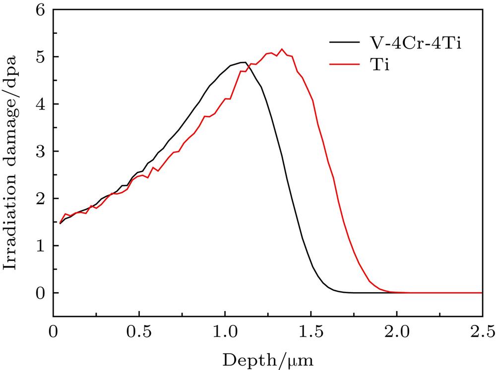
    Fig. 1. Irradiation damage (dpa) in V-4Cr-4Ti/Ti samples calculated by SRIM2008 software.由SRIM软件计算得到的V-4Cr-4Ti和Ti的辐照损伤随样品深度的变化
    The SEM morphology and EDS line analysis of V-4Cr-4Ti/Ti samples: (a) Before and (b) after irradiation; the positions of FIB samples are marked with white rectangles.V-4Cr-4Ti/Ti界面区域及两侧基体在(a) 辐照前和 (b) 辐照后的SEM形貌图及对应的EDS元素线扫描分析结果; 图中的白色长方形区域为FIB的取样位置
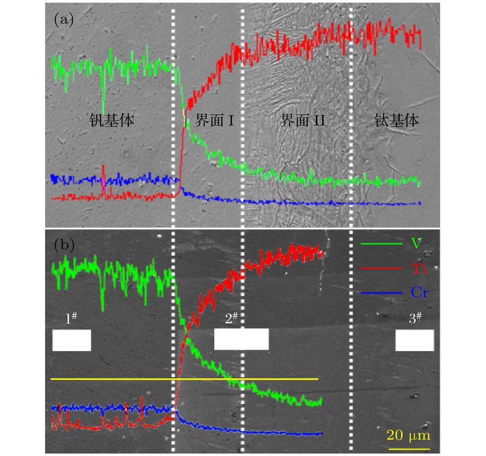
    Fig. 2. The SEM morphology and EDS line analysis of V-4Cr-4Ti/Ti samples: (a) Before and (b) after irradiation; the positions of FIB samples are marked with white rectangles.V-4Cr-4Ti/Ti界面区域及两侧基体在(a) 辐照前和 (b) 辐照后的SEM形貌图及对应的EDS元素线扫描分析结果; 图中的白色长方形区域为FIB的取样位置
    Vickers hardness distribution across the interface of the V-4Cr-4Ti/Ti.V-4Cr-4Ti/Ti界面及两侧基体区域的硬度分布
    Fig. 3. Vickers hardness distribution across the interface of the V-4Cr-4Ti/Ti.V-4Cr-4Ti/Ti界面及两侧基体区域的硬度分布
    The TEM images of V-4Cr-4Ti/Ti after irradiation: (a) V-4Cr-4Ti; (b) interface I; (c) interface II; (d) Ti.V-4Cr-4Ti/Ti界面区域及两侧基体辐照后的TEM形貌图 (a) 钒基体; (b) 界面I; (c) 界面II; (d) 钛基体
    Fig. 4. The TEM images of V-4Cr-4Ti/Ti after irradiation: (a) V-4Cr-4Ti; (b) interface I; (c) interface II; (d) Ti.V-4Cr-4Ti/Ti界面区域及两侧基体辐照后的TEM形貌图 (a) 钒基体; (b) 界面I; (c) 界面II; (d) 钛基体
    Dislocation density (a) and diameter (b) distribution across the interface.辐照后V-4Cr-4Ti/Ti界面及两侧基体的位错密度(a) 和尺寸 (b)
    Fig. 5. Dislocation density (a) and diameter (b) distribution across the interface.辐照后V-4Cr-4Ti/Ti界面及两侧基体的位错密度(a) 和尺寸 (b)
    STEM images of V-4Cr-4Ti/Ti interface after irradiation: (a) V-4Cr-4Ti; (b) interface I; (c) interface II.辐照后界面处的STEM形貌图 (a) 钒基体; (b) 界面I; (c) 界面II
    Fig. 6. STEM images of V-4Cr-4Ti/Ti interface after irradiation: (a) V-4Cr-4Ti; (b) interface I; (c) interface II.辐照后界面处的STEM形貌图 (a) 钒基体; (b) 界面I; (c) 界面II
    EDS analysis of the V-4Cr-4Ti/Ti: (a) Interface before irradiation; (b) V-4Cr-4Ti after irradiation; (c) interface I after irradiation; (d) interface II after irradiation.辐照前后析出物EDS分析结果 (a) 辐照前界面; (b) 辐照后钒基体; (c) 辐照后界面I; (d) 辐照后界面II
    Fig. 7. EDS analysis of the V-4Cr-4Ti/Ti: (a) Interface before irradiation; (b) V-4Cr-4Ti after irradiation; (c) interface I after irradiation; (d) interface II after irradiation.辐照前后析出物EDS分析结果 (a) 辐照前界面; (b) 辐照后钒基体; (c) 辐照后界面I; (d) 辐照后界面II
    EDS-mapping analysis of the V-4Cr-4Ti and interface I after irradiation: (a)−(d) V-4Cr-4Ti; (e)−(h) interface I.辐照后钒基体和界面I处析出物EDS面扫描分析结果 (a)—(d) 钒基体; (e)—(h) 界面I
    Fig. 8. EDS-mapping analysis of the V-4Cr-4Ti and interface I after irradiation: (a)−(d) V-4Cr-4Ti; (e)−(h) interface I.辐照后钒基体和界面I处析出物EDS面扫描分析结果 (a)—(d) 钒基体; (e)—(h) 界面I
    Diffraction analysis of irradiated samples: (a) V-4Cr-4Ti; (b) Ti; (c), (d) interface I; (e) (f) interface II.辐照后样品不同区域的选区电子衍射分析结果 (a) 钒基体; (b) 钛基体; (c), (d) 界面I; (e), (f) 界面II
    Fig. 9. Diffraction analysis of irradiated samples: (a) V-4Cr-4Ti; (b) Ti; (c), (d) interface I; (e) (f) interface II.辐照后样品不同区域的选区电子衍射分析结果 (a) 钒基体; (b) 钛基体; (c), (d) 界面I; (e), (f) 界面II
    钒基体界面I界面II钛基体
    注: *表示界面II处α + β Ti区的硬化按α-Ti和β-Ti各占50%进行计算.
    ΔHV实验值20713655247
    N/m–31.5 × 10228.0 × 10218.4 × 10211.3 × 1022
    d/nm7.3 ± 1.519.9 ± 5.020.3 ± 4.811.2 ± 2.0
    N·d1.09 × 10141.59 × 10141.70 × 10141.46 × 1014
    $ \sqrt {N\cdot d} $1.05 × 1071.26 × 1071.31 × 1071.21 × 107
    ΔHV计算值39.527.738.6*44.8
    Table 1.

    Experimental hardness values by nanoindentation and the estimated hardness values calculated by the DBH model

    通过纳米压痕所得硬化实验值与采用DBH模型对辐照硬化进行的估算值

    Ran-Ran Li, Yi-Fan Zhang, Dian-Cheng Geng, Gao-Wei Zhang, Hideo Watanabe, Wen-Tuo Han, Fa-Rong Wan. Characterization of interface irradiation damage in Ti-clad V-4Cr-4Ti composite material[J]. Acta Physica Sinica, 2019, 68(21): 216101-1
    Download Citation