Key Laboratory for Advanced Functional Materials of the Ministry of Education, College of Materials Science and Engineering, Beijing University of Technology, Beijing 100024, China
Graphene has attracted great interest in optoelectronics, owing to its high carrier mobility and broadband absorption. However, a graphene photodetector exhibits low photoresponsivity because of its weak light absorption. In this work, we designed a graphene/ heterostructure photodetector, which exhibits photoresponse ranging from visible to near infrared and an ultrahigh photoresponsivity up to at 550 nm. The electron–hole pairs are excited in a few-layered and separated by the built-in electric field. A large number of electrons shift to graphene, while the holes remain in the , which creates a photogating effect.
Nowadays, significant attention has been paid to graphene because of its wide application in many optoelectronic devices[1–5]. Numerous features, like a unique zero gap band structure and an extremely wide absorption spectrum, make graphene an extremely appropriate material for broadband and ultrafast photodetection[6–8]. However, its weak light absorbance and quick recombination of a photoexcited carrier (several picoseconds) result in low responsivity () of its photodetector, which will limit its application in video imaging[7,9,10].
In order to solve the above problems, novel optical structures and other materials are combined with graphene. Metamaterials and microcavities are two common types of structures integrated with a graphene photodetector to raise its photoresponsivity, owing to the large absorption of the incident light. Nevertheless, the photoresponsivity is only increased by an order of magnitude, and the resonant frequency is confined to a few wavelengths of light[11–13]. Besides, quantum dots and perovskites have been applied to promote the performance of graphene photodetectors, which improve the photoresponsivity of several orders of magnitude[14,15]. However, the stability and toxicity of those materials deserve to be further studied, and the preparation processes are complicated.
In recent years, heterostructures composed of graphene and transition metal dichalcogenides (TMDs)[16], such as films, are able to enhance photodetection efficiency, as they take advantage of the high carrier’s mobility of graphene and large amounts of photoexcited carriers in TMDs. Due to a wide bandgap of those TMDs, the application of this kind of photodetector is limited in the visible light range (for example, monolayer , 1.8 eV; , 1.6 eV; and , 2.1 eV)[17]. Although single-layer is a direct band structure with the bandgap of 1.5 eV, its bulk form shows an indirect bandgap of 1.1 eV, which expends its application in near-infrared (NIR) regime. Recently, several attempts of photodetectors based on in the visible spectrum range have been demonstrated[18,19]. For example, a multi-layered (20 nm) photodetector was measured at 532 nm and responsivity achieves . Unfortunately, this result was only obtained with a gate voltage of 20 V and a drain–source voltage of 8 V, which has limited use in practical applications and shows high energy consumption. As far as we know, no experiment results about acceptable responsivity in the NIR range are reported from previous investigations of photodetectors. Therefore, it is worth developing an NIR photodetector consisting of graphene and with high responsivity and low energy consumption.
Sign up for Chinese Optics Letters TOC. Get the latest issue of Chinese Optics Letters delivered right to you!Sign up now
In this work, a van der Waals graphene/ heterostructure photodetector is proposed, in which few-layered and monolayer graphene work as the absorptive layer and channel layer, respectively. The electron–hole pairs are separated, and holes remain in , while the built-in electric field between graphene and drives electrons flowing into graphene . The lifetime of electrons can be greatly extended, because the trap of holes in delays the recombination in the circuit, which is the photogating effect on a graphene photodetector. With this ingenious design, the photoresponsivity of the heterostructure photodetectors can achieve at 550 nm and at 950 nm, which is much larger than the value of pure graphene or .
Graphene and were peeled separately on a silicon substrate with a 300 nm thick oxide layer and commercial poly(dimethylsiloxane) (PDMS). Then, a few-layered flake on the PDMS was stacked onto a monolayer graphene flake. A transport channel of the device was patterned first by UV lithography technology (SUSS MJB4). Then, the two metal contacts of Ti/Au (10 nm/80 nm) at each end of the graphene flake were fabricated by the e-beam evaporation system (HHV FL400).
Raman spectra and mapping were recorded with a Witec alpha 300 conformal Raman microscope using 532 nm laser excitation. The laser spot size is around μ. The Raman mapping area for samples is about μμ, with a step size of μ in each direction. The thickness and the surface potential of the heterostructure were measured with a Bruker MultiMode 8 atomic force microscope (AFM). A semiconductor device analyzer (Agilent B1500 A) was employed to measure all of the electric and optoelectronic properties of the device in ambient air. The illumination light was obtained by the SuperK EXTREME supercontinuum white light laser, and monochromatic light was selected through a monochromator (from 450 to 1000 nm). The light spot size was focused by a Nikon Ni-U microscope.
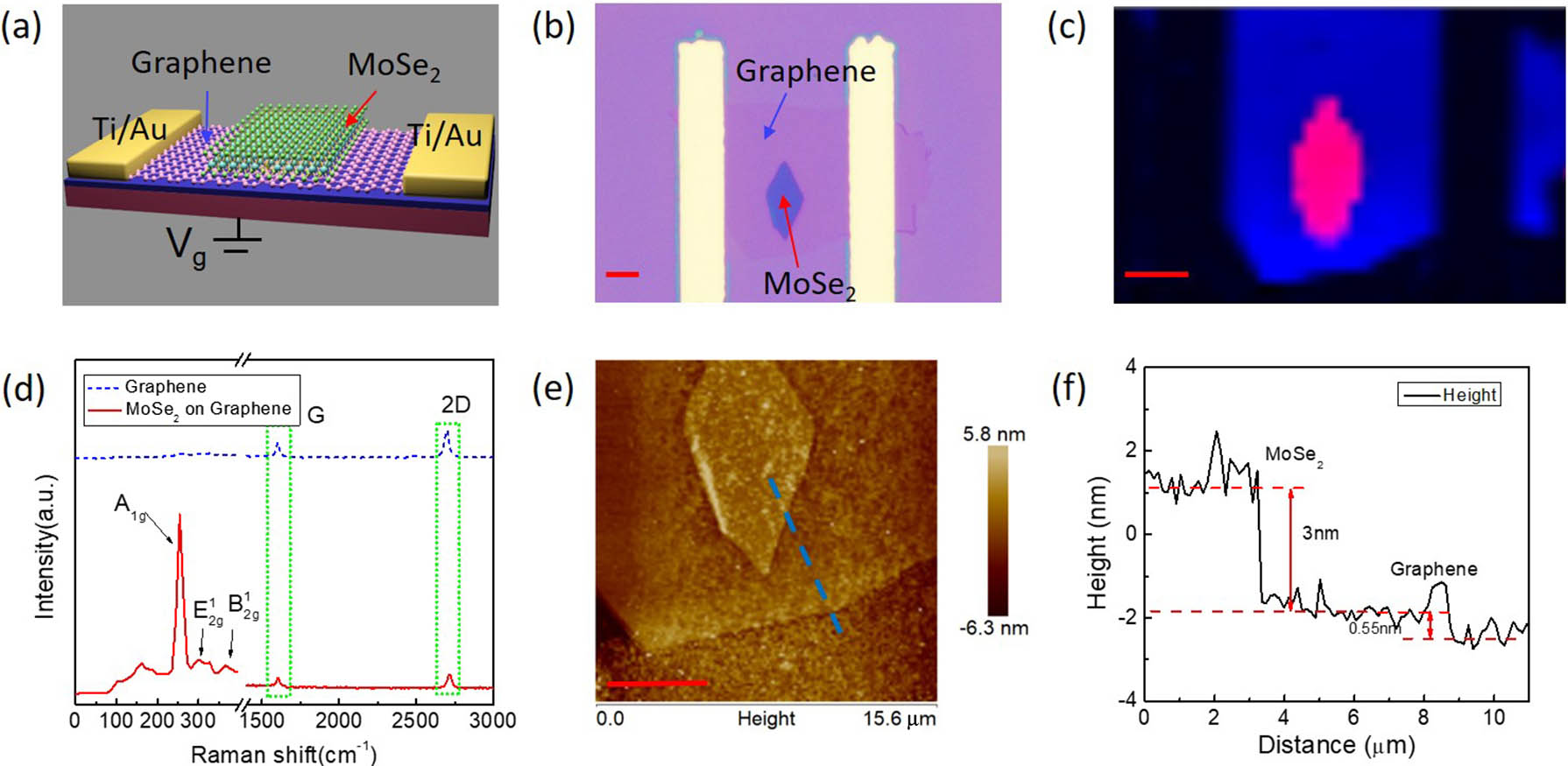
Figures 1(a) and 1(b) display a schematic of the vertical /graphene heterostructure device and an optical image. The flake was transferred to the surface of the graphene flake, and two electrodes were deposited on the heterostructure as a source and drain. The device is added with a gate bias through the highly doped silicon substrate and is illuminated from the top during photoelectric testing. Figure 1(c) shows combined Raman mapping at (blue area) of and (red area) of graphene. The result displays the overlap area of graphene and , confirming the formation of the vertical heterostructure of graphene and . Figure 1(d) illustrates the Raman spectra of graphene and graphene/ heterostructure excited at 532 nm. The positions of the G band and two-dimensional (2D) band of graphene, which are detected at around 1584 and , and the intensity ratio of the 2D band and the D band () are in accordance with the characteristics of single-layer graphene[20]. Two Raman vibration modes of , which are characteristic out-of-plane and in-plane , are observed at around 242 and , respectively. In addition, the peak at about is a bulk Raman inactive mode of , which always appears in few-layered flakes[21,22]. Figure 1(e) displays the AFM morphology of the graphene/ heterostructure. Figure 1(f) presents the thickness of and graphene, which is 3 and 0.5 nm, respectively. is about four layers and graphene is one layer, which is consistent with the results of the Raman spectra.
Figure 1.(a) Schematic diagram of the /graphene photodetector, (b) optical image of the heterostructure device, (c) Raman mapping, (d) Raman spectrum of the graphene and /graphene heterostructure, (e) AFM morphology of the /graphene heterostructure, and (f) thickness of graphene and . Scale bar, μ.
Figure 2(a) displays the output characteristic curves of the graphene/ heterostructure device in dark state and under various light power. While applying a small drain voltage (, ), the graphene/ heterostructure shows a remarkable decrease with increase of the light power. In contrast, tuning the gate voltage to 80 V, output characteristic curves appear as opposite phenomenon that currently rises with an increase of the light power, as illustrated in Fig. 2(b). This phenomenon needs to be explained in combination with the transfer curve. Figure 2(c) depicts the transfer curve of the -type doping transport characteristics in the absence of light, since a typical Dirac point (the charge neutrality point) is about 80 V. Noteworthily, under light illumination, shifts to lower voltage () with a light power increase to 143 nW, suggesting that the photoexcited electrons transferred into graphene. In particular, as is more sensitive to the incident light, a large number of the electron–hole pairs emerge in it. Driven by the coulomb force, the electron–hole pairs are separated promptly at the /graphene interface, then electrons shift to graphene, and the holes are captured by , resulting in a photogating effect. To be specific, the acts as a gate by capturing the holes under illumination, which leads to the change of carrier density in graphene under light conditions. Because electrons in graphene travel at a ultrafast speed, they do not recombine with holes in until they circulate in the circuit for plenty of times. Therefore, the above factors greatly enhance the photoresponse. Figure 2(d) exhibits a photocurrent varying with gate voltage under various light power, where the photocurrent is defined as . It is obvious in the graph that photocurrent can be tuned by the gate voltage and increases with the light intensity. With gradually tuning the gate voltage from to 80 V, the Fermi level of graphene rises from the valence band to the conduction band. When applying , carriers in the graphene channel are holes. Under illumination, photoexcited electrons are injected to the channel, resulting in a negative photocurrent, as displayed in Fig. 2(a). After , as electrons become dominant carriers in the channel, the photocurrent changes from negative to positive. That indicates the tunable feature can control the on–off switching state of the device, resorting to the ambipolar property of graphene.
Figure 2.Output curves at various input light: (a) and (b) . (c) Transfer curves at light off and on, . (d) Photocurrent varying with gate voltage under various light power. Incident light, 550 nm.
In order to thoroughly investigate the mechanism and the band bending of this heterostructure, surface potential of this heterostructure was measured by means of Kelvin probe force microscopy (KPFM). Figure 3(a) shows a KPFM image of our heterostructure, and a profile of the surface potential along the blue dashed line in Fig. 3(a) is shown in Fig. 3(b). Here, different surface potential between graphene and is revealed. According to the equation , the contact potential difference () can be calculated by the difference of the work function between the sample and the probe, which is noted as and , respectively. As the surface potential of is much higher than the one of graphene, which is shown in Fig. 3(b), the Fermi energy of is lower before the contact. The corresponding band structure is depicted in Fig. 3(c). Moreover, the difference of Fermi energy between these two materials causes band bending of in the area adjacent to graphene to decrease slightly, and an internal electric field points from graphene to . When is driven by this electric force, the electrons move to graphene, and the holes stay in , where the photoexcited electron–hole pairs are generated under illumination. Therefore, the density of holes in graphene reduces, which leads to the lower channel current. Applying gate voltage , as the photoelectrons still inject into graphene, the density of electrons increases dramatically, which results in the enhancement of the current.
Figure 3.(a) KPFM image of graphene/ heterostructure; scale bar, μ. (b) Surface potential between graphene and . (c) Band diagram of graphene and before contact under dark. After they are in contact, the Fermi level is aligned, and the band bending of in the area adjacent to graphene decreases slightly. Band diagram of graphene and under light illumination, (d) and (e) . Blue dashed lines represent the Fermi level.
To further study the optoelectronic performances, responsivity of the graphene/ heterostructure device varying against wavelength and light power was measured. The responsivity R can be calculated from the equation where and are the photocurrent and light power shed on the device, respectively. The above results are shown in Fig. 4(a), varying the wavelength from 450 to 1000 nm with an interval of 50 nm. The device was tested in ambient air with , . A peak responsivity (up to ) is observed at about 550 nm, and then it gradually drops to at 950 nm. Distinctively, the photoresponse spectrum of our device corresponds well to the bandgap and absorption of in previous reports[21,23]. These results demonstrate that on graphene surfaces is indispensable in the photocurrent generation in our device. Besides, the responsivity is at 450 nm. Therefore, it can be judged from the trend that the shorter wavelength will also have a certain response.
Figure 4.(a) Responsivity of the graphene/MoSe2 heterostructure photodetector varying with the wavelength from 450 to 1000 nm. (b) Responsivity varying with light power, and the curve can be fitted by the equation . Blue dots represent experimental data, and the red dashed line is the fitting curve: , .
The responsivity reduces dramatically with an increase in the light power, as shown in Fig. 4(b), and the curve can be fitted by the equation , where is a characteristic index to judge the photogating effect[24]. For the traditional photoconductive detectors, the photocurrent has a linear relation with the incident light power before saturated absorption and , where the power exponent is equal to 1 or very close to 1. By contrast, for the 2D materials photodetector, the complex process of carrier generation, trapping, and recombination within semiconductors result in a higher photocurrent under same light power. Thus, a nonunity exponent of can be found, and the gain caused by the photogating effect would increase with close to 0. Remarkably, such a photogating effect is responsible for the high responsivity of our photodetector, which is more than with a light power of 0.57 nW at , . If the light intensity is lower, the maximum responsivity can be increased by an order of magnitude or more. This responsivity is several orders of magnitude higher than the one in graphene (6.1 mA/W) and the (97.1 A/W) phototransistor reported before[7,18]. Similar to our device, some -based photodetectors reach high responsivity by the photogating effect[25–27]. However, the difference is that these detectors trap the carriers by a back gate, floating gate, or ferroelectrics film gate rather than of our device.
The time-dependent photocurrent was measured for illumination of the wavelength at 550 nm, which is displayed in Fig. 5. An exponential function with relaxation time can be applied to fit the curve as the photocurrent decreases under the illumination ·(), where the time constant is about 22 s. When trap states in the interface between graphene and are filled, the photoelectrons will be transferred to the graphene channel, leading to slow photoresponse. However, the response time can be reduced from tens of seconds down to a few milliseconds or even shorter by decreasing the electron trap lifetime of the material because it can be controlled through promoting its quality and reducing the densities of defects[28].
Figure 5.Time-dependent photocurrent of the graphene/ heterostructure device, and the time constant is about 22 s.
In this work, we successfully prepared a graphene/ vertical heterostructure photodetector. The channel layer is graphene, while the , which acts as a light absorption layer, generates the photogating effect by introducing trap states for photoexcited holes. Photoconductors relying on such a photogating effect can obtain large gain because the accumulated holes act as a positive gate and electrons act as charge carriers in the device. Our photodetector shows high responsivity ranging from 450 to 1000 nm, and an ultrahigh photoresponsivity can achieve at 550 nm. This work demonstrates that this new type of heterostructure between graphene and other narrow band structure 2D materials will enhance the sensitivity and other indices of the photodetector, which proposes an efficient solution for the difficulties in design and application of optoelectronic devices.