Abstract
We present a technique for fabricating a fluorescence enhancement device composed of metal nanoparticles (NPs) and porous silicon (PSi) diffraction grating. The fluorescence emission enhancement properties of the PSi and the fluorescence enhancement of the probe molecules are studied on PSi gratings. The fluorescence enhancement of the probe molecules on a fluorescence enhancement device is further improved through the deposition of metal NPs onto the PSi grating. In comparison to metal NP/PSi devices, metal NP periodic distributions can produce a stronger fluorescence enhancement that couples with the PSi grating fluorescence enhancement to achieve an overall three-fold enhancement of the fluorescence intensity.Fluorescence enhancement as an extensive subject of research has great potential application in the fields of biological sensors, tracking analysis, and more. The realization of a highly sensitive fluorescence enhancement is closely related to the enhancement of near-field optical energy and the quantum yield. To effectively gather light energy in close proximity to a surface area and further realize photon energy transfer, the surface plasmon resonance (SPR) properties of metal nanoparticles (NPs) are required[1–4]. Such an enhanced fluorescence can be achieved when metal NPs are deposited onto a suitable substrate[5–8]. However, the aggregation of the metal NPs on the surface of a substrate is not controllable, which can lead to poor fluorescence enhancement reproducibility and greatly limits applications. In order to effectively control the fluorescence enhancement substrate field distribution uniformity and repeatability, metal NPs must be arranged in an ordered manner on different substrate materials as a usual method[9–11] or deposited onto a thin metal layer on a fixed template[12,13]. These templates can be fabricated using different techniques like electron beam evaporation[9], electron beam lithography[11], imprint lithography[13,14], and holography[15]. The productive periodic structure of the templates results in a higher fluorescence signal intensity and a more uniform signal. In particular, highly ordered metallic gratings (Au, Ag) are able to excite surface plasmon polaritons (SPPs)[16]. SPPs are capable of gathering light energy in a region close to the surface. In this case, the metal grating substrate can enhance the fluorescence resonance of the detection objects adsorbed on the surface of the substrate.
The huge specific surface area of porous silicon (PSi) increases the deposition rate of the detection objects, which can improve the fluorescence signal intensity[17–20]. The substrate system combined with PSi and metal NPs excites SPR, which has the capability of enhancing the fluorescence of adsorbed detection objects. The coupling of the enhanced fluorescence caused by the use of PSi and the enhanced fluorescence resulting from use of the metal grating is expected to produce the greatest fluorescence enhancement response.
In this Letter, we present a fluorescence enhancing device composed of metallic NPs and a PSi grating. The PSi grating improves the fluorescence emission properties of the PSi and enhances the fluorescence signal intensity of the detected object molecules adsorbed onto the PSi grating device. The detection object fluorescence signal intensity is further enhanced with the addition of metal NPs onto the PSi grating device. The PSi grating periodic structure is conductive to improve the metal NPs distribution uniformity, and to ameliorate the fluorescence detection signal uniformity and repeatability. This metal NP/PSi grating device is expected to be applied in highly sensitive biological detection.
Sign up for Chinese Optics Letters TOC. Get the latest issue of Chinese Optics Letters delivered right to you!Sign up now
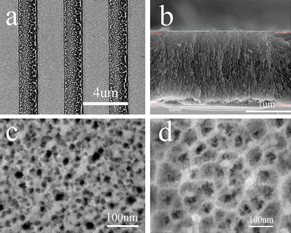
The rectangular groove silicon grating was fabricated with p-type monocrystalline silicon<100> (resistivity ), using photolithography techniques. The period of the grating is 4 μm. The grating surface morphology is shown in Fig. 1(a); note that the groove depth is 30 nm. Planar PSi and the PSi grating were prepared using a electrochemical etching current density, with a 30 s corrosion time and a corrosion area. The etching solution is a mixture of hydrofluoric acid (40%) and alcohol (1:1, v/v). All samples were properly cleaned with deionized water (DI water) and dried at room temperature. Figure 1(b) shows the PSi grating cross section. The high and low relief structures of the surface, as well as the bottom of the PSi grating, can be clearly observed. The partially enlarged surface morphology images of the ridge and the groove are shown in Figs. 1(c) and 1(d), respectively. The average pore diameter is roughly 30 nm.

Figure 1.(a) Top view of the PSi grating, (b) the cross section of the PSi grating; the partially enlarged surface morphology of (c) the ridge and (d) the groove.
PSi and PSi grating samples were passivated in a 30% hydrogen peroxide solution for 12 h at room temperature, rinsed with DI water, and dried in air. The passivated PSi samples were immersed in (3-aminopropyl) triethoxysilane (APTES, 5%) at room temperature for 1 h, then rinsed with DI water, and allowed to dry.
Ag NPs were prepared using the chemical reduction method. The silver nitrate (50 mL, 1.0 mmol/L) solution was heated to boiling using a heat collection-type magnetic heating agitator. While boiling, a sodium citrate aqueous solution (8 mL, 1 wt%) was rapidly added until the solution color changed from colorless to yellow-brown.
The solution was then cooled to room temperature. The UV–Vis absorption spectrum of Ag NPs is shown in Fig. 2(a). The strongest absorption peak is located at 417 nm, and the average particle diameter is 30 nm. Both the PSi gratings and the planar PSi samples were soaked in the colloidal silver solution for 8 h. Metal NPs adsorb onto the pore walls through electrostatic adsorption.
Figure 2.UV–Vis absorption spectra of (a) Ag NPs and (b) Au NPs.
The Au NP synthesis procedure is to heat chloroauric acid solution (50 mL, 1 mmol/L) to boiling, and then quickly add a sodium citrate solution (2 mL, 1 wt%) until the solution changes from yellow to dark red. The size of the Au NPs is approximately 10 nm, as presented in the literature[19]. The UV–Vis absorption spectrum of an Au NP solution is shown in Fig. 2(b). The strongest absorption peak is located at 522 nm. The Au NP solution (25 mL) was centrifuged for 20 min at 12,000 rpm. After removing the supernatant (23 mL), the solution was diluted with alcohol to 0.5 mg/mL. Ten drops of Au NP solution (the total amount of 1 mL) were dripped onto the PSi grating. The samples were then dried in a constant temperature chamber at 37°C and drop out after drying.
Before measurement, rhodamine 6 G (R6 G) (100 nmol/L) was dropped onto both the Ag NP (Au NP)/PSi grating and the Ag NP (Au NP)/planar PSi, and was allowed to dry.
Fluorescence intensities were obtained with a UV–Vis fluorescence spectrophotometer (Hitachi F-4600, Japan). The slit width was 5 nm, the excitation power was 700 mW, the response time was 0.004 s, and the data were collected from five different locations on the same sample and averaged. The reflection spectroscopy data were collected using a UV–Vis spectrometer (U-4100 Hitachi, Japan). A field emission scanning electron microscope (SUPRA55 VP ZEISS, Germany) was used to measure the morphology.
The preparation process for the metal NP/PSi grating fluorescence enhancement system is presented in Fig. 3. The fluorescence enhancement system consists of grating, a single layer of PSi, and metal NPs. The silicon grating is fabricated using microlithography techniques; the grating period is 4 μm. The PSi grating is fabricated using electrochemical corrosion; the surface morphology is shown in Fig. 1. After fabricating the PSi grating, the metal NPs (Ag NPs and Au NPs) were assembled onto the PSi grating to form a metal NP/PSi grating fluorescence enhancement device. The metal NPs were uniformly dispersed onto/in the PSi grating, forming a device with a metallic NP diffraction grating to effectively stimulate surface plasma. Light energy was gathered near the surface, which increased the number of probe molecules in the excited state and improved the fluorescence quantum yield. As a result, the fluorescent signal from the R6 G molecules adsorbed on the surface was enhanced.
Figure 3.Schematic diagram of the preparation of a metal NP/PSi grating fluorescence enhanced device system.
Figure 4 shows the reflection spectrum at a normal incidence for both the rectangular groove grating with a 30 nm depth and the planar crystal silicon. The rectangular groove grating scattering effect increases the photon propagation path and the incident light absorption. Meanwhile, diffraction effects result in a spectrum broadening of the emergent light relative to the incident light. In addition to vertically diffracted light, light is diffracted along other directions. As a result, the grating has a lower reflection compared to a planar surface. The reflection decrease is favorable to the grating transmission performance improvement and the light energy capture rate, which is ultimately desired for preparing high performance devices.
Figure 4.Reflection spectra of a rectangular groove silicon grating and a planar crystal silicon. The grating groove depth is 30 nm.
Figure 5(a) shows the reflection spectra for a PSi grating and a planar PSi. There are obvious interference peaks from the PSi grating and the planar PSi; the PSi grating reduces the reflectivity due to diffraction and scattering. The PSi grating cross section is shown in Fig. 3. Note the high and low relief structure, which can be considered a grating composed of PSi and air, and a composite grating composed of monocrystalline silicon and PSi. The transmission performance improvement results in incident light penetrating into the deeper layer. The increased interaction length improves the incident light absorbance. Fluorescence is emitted after the material absorbs optical or other electromagnetic energy; the enhanced PSi grating absorption results in an increasing number of excited state photons, which eventually leads to an increased transition probability. For a given excitation intensity, this greater transition probability produces a fluorescence enhancement effect, as shown in Fig. 5(b), and the exciting wavelength is 380 nm.
Figure 5.PSi grating and planar PSi device (a) reflection spectra and (b) fluorescence spectra.
Figure 6 shows the R6 G (100 nmol/L) fluorescence spectra on different substrates, the exciting wavelength is 500 nm. When the same R6 G concentration was deposited onto the surface of the silicon grating and planar monocrystalline silicon, the R6 G fluorescence signal was hardly observed on the planar silicon surface. For a smooth plane, rhodamine molecules are difficult to adsorb on the surface and easily aggregate to produce self-quenching. In addition, a weak signal was observed on the silicon grating surface. The grating structure can regulate the strong aggregation of rhodamine molecules, improve the dispersion, and enhance the interaction time between the light and rhodamine molecules, resulting in fluorescence enhancement. After the PSi preparation, the presence of pores’ greater distance between molecules can avoid or minimize the problem of self-quenching of fluorescence, and the large specific surface area results in increased R6 G deposition, enhancing the fluorescence signal. The observed R6 G fluorescence signal intensity on the PSi grating device was significantly higher than the R6 G fluorescence signal intensity on the planar PSi. This phenomenon is primarily due to the PSi grating enhanced transmission and optical absorption, which effectively increases the fluorescent molecule quantum yield. The fluorescence enhancement effect in the PSi grating and the planar PSi device combined with the metal NPs is greatly improved compared with that of nonmetallic NPs. The metal NP periodic distribution serving as a metal NP diffraction grating effectively excites SPPs, which gather light energy near the surface. This ultimately enhances the R6 G fluorescence intensity. The fluorescence intensity of the R6 G on the (Ag NP)/PSi grating device is three times larger than the fluorescence intensity of the R6 G on an (Ag NP)/PSi device.
Figure 6.(Color online) Fluorescence spectra of R6 G (100 nmol/L) on different substrates. The insert map presents the fluorescence intensity of R6 G (100 nmol/L) detected on rectangular groove silicon grating and smooth silicon.
To verify the fluorescence signal uniformity and repeatability, the enhanced R6 G fluorescence signal was also obtained for Au NPs assembled onto a PSi grating device (in Fig. 7) with an exciting wavelength 500 nm.
Figure 7.Fluorescence spectra of R6 G (100 nmol/L) on a metal NP/PSi grating device.
In this Letter, we study fluorescence emission enhancement using a PSi grating. We demonstrate R6 G fluorescence enhancement on a metal NP/PSi grating device. PSi with a grating structure can enhance fluorescence emission; the fluorescence signal intensity is doubled in comparison to that of a planar PSi device. Metal NPs are deposited onto a PSi grating and a planar PSi substrate, which effectively enhance the R6 G fluorescence signal intensity. The combination of a metal NP grating and a PSi device can achieve the most efficient light energy aggregation in the near-surface region, resulting in a strong fluorescence signal enhancement. The R6 G enhanced fluorescence signal intensity on an Ag NP/PSi grating device is 3 times larger than the intensity on an Ag NP/planar PSi device.
References
[1] K. Sokolov, G. Chamanov, T. M. Cotton. Anal. Chem., 70, 3898(1998).
[2] K. Aslan, I. Gryczynski, J. Malicka. Curr. Opin. Biotechnol., 16, 55(2005).
[3] S. Ekgasit, F. Yu, W. Knoll. Sens. Actuators B., 104, 294(2005).
[4] Y. Chen, Z. Li. Chin. Opt. Lett., 13, 020501(2015).
[5] C. D. Geddes. Angular-dependent metal-enhanced fluorescence(2007).
[6] M. Pelton, J. Aizpurua, G. Bryant. Laser Photon. Rev., 2, 136(2008).
[7] T. K. Sau, A. L. Rogach, J. Frank, T. A. Klar, J. Feldmann. Adv. Mater., 22, 1805(2010).
[8] J. Kottmann, O. Martin, D. Smith, S. Schultz. Opt. Express., 6, 213(2000).
[9] P. Pavaskar, I. K. Hsu, J. Theiss, W. H. Hung. J. Appl. Phys., 113, 034302(2013).
[10] , P. Tiwari, S. Bhartiya, C. Mukherjee, M. N. Singh, A. K. Sinha. J. Appl. Phys., 118, 064303(2015).
[11] B. Yan, A. Thubagere, W. R. Premasiri, L. D. Ziegler, L. D. Negro, B. M. Reinhard. ACS Nano, 3, 1190(2009).
[12] M. Kahraman, P. Daggumati, O. Kurtulus, E. Seker, S. Wachsmannhogiu. Sci. Rep., 3, 3396(2013).
[13] M. Geissler, K. Li, B. Cui, L. Clime, T. Veres. J. Phys. Chem. C, 113, 17296(2009).
[14] A. Kocabas, G. Ertas, S. S. Senlik, A. Aydinli. Opt. Express, 16, 12469(2008).
[15] Y. Li, H. Chen, S. Kroker, T. Käsebier, Z. Liu, K. Qiu, Y. Liu, E.-B. Kley, X. Xu, Y. Hong, S. Fu. Chin. Opt. Lett., 14, 090501(2016).
[16] M. G. Banaee. ACS Nano, 5, 307(2010).
[17] Y. Jiao, D. S. Koktysh, N. Phambu, S. M. Weiss. Appl. Phys. Lett., 97, 153125(2010).
[18] M. B. D. L. Mora, J. Bornacelli, R. Nava, R. Zanella, J. A. Reyes-Esqueda. J. Lumin., 146, 247(2014).
[19] F. Shi, Z. Jia, X. Lv, J. Zhou. Phys. Status Solidi A, 212, 662(2014).
[20] L. He, Z. Jia, J. Zhou. Chin. Opt. Lett., 14, 041601(2016).