Author Affiliations
1Beijing National Laboratory for Condensed Matter Physics, Institute of Physics, Chinese Academy of Sciences, Beijing 100190, China2CAS Center for Excellence in Topological Quantum Computation and School of Physical Sciences, University of Chinese Academy of Sciences, Beijing 100049, China3Songshan Lake Materials Laboratory, Dongguan 523808, Chinashow less
Semiconductor quantum dots (QDs) are usually recognized as “artificial atoms” that have discrete states due to the quantum confinement of electrons and holes in three dimensions. Several methods have been developed for growing QDs, in which the self-assembled QDs grew by Stranski-Krastanov method possess superior optical properties, including high radiative efficiency and high purity of single photon emission. Benefiting directly from the advanced semiconductor growth and processing technologies, the QDs are able to be integrated with a wealth of photonic nanostructures, which can be implemented in the research field of solid-state quantum electrodynamics.
On one hand, the coupling between QDs and photonic nanostructures can modify the properties of QDs, such as spontaneous emission rate. On the other hand, the strong coupling will entangle the light-matter degrees of freedom leading to the formation of polariton. Both have widespread and far-ranging applications in the development of cutting-edge quantum technologies, including photonic quantum information processing, quantum key distribution and integrated quantum optical circuits. In the past decades, numerous works have investigated the coupling of QDs to various photonic nanostructures[1], especially the coupling to photonic crystal cavity and waveguide which brings this platform one step closer toward realization of spin-photon quantum interface and on-chip integrated quantum photonics, as shown in Fig. 1.

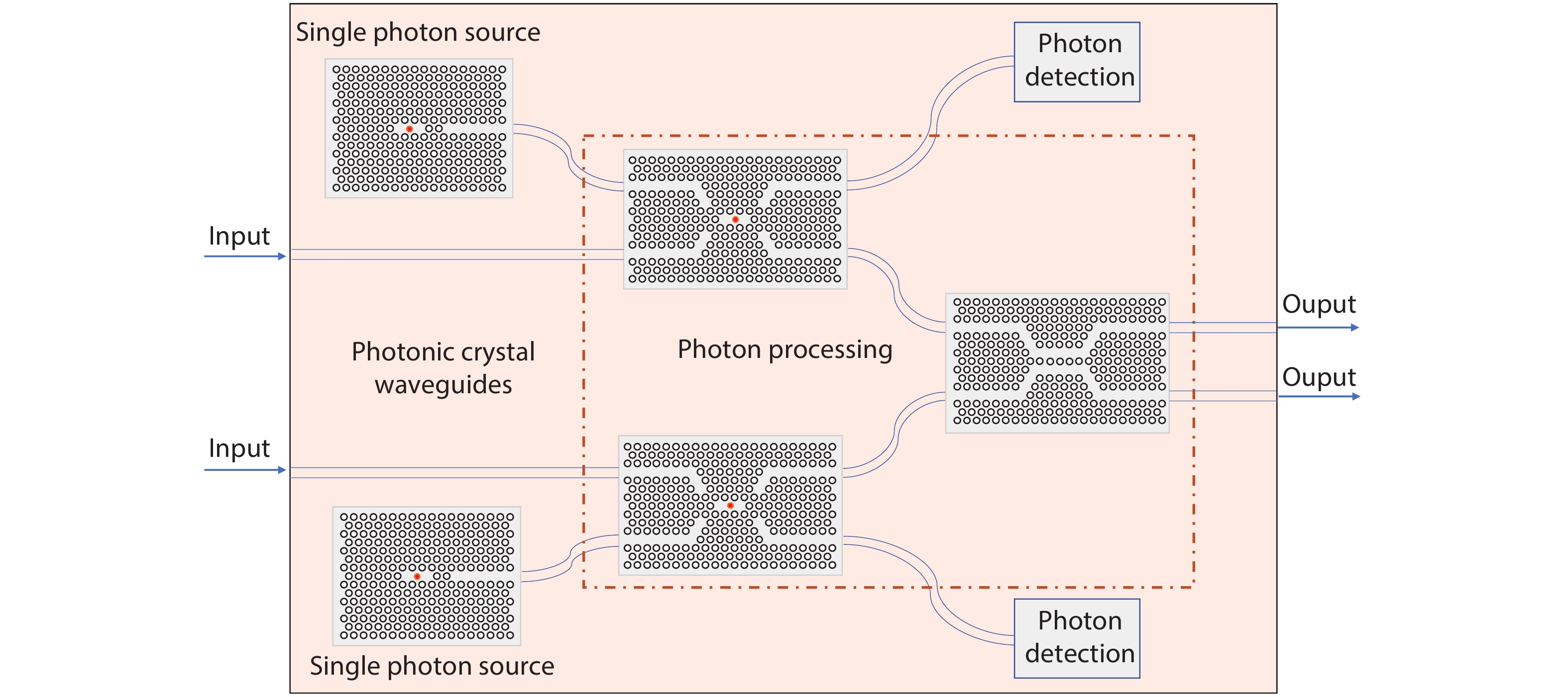
Figure 1.(Color online) Schematic of on-chip integrated quantum photonic circuitry. The red points indicate the QDs in photonic crystal structures.
The interactions between QDs and photonic crystal cavities have been thoroughly investigated, which can be divided into weak and strong coupling regimes. In the weak coupling regime, where the coupling strength g is smaller than the decay rate of the system κ, the spontaneous rate of QDs can be greatly enhanced according to Purcell effect. It has been proposed and demonstrated for the realization of high-efficient single photon source[2] and ultrafast qubit gates[3]. In the strong coupling regime, where g is larger than κ, a cavity polariton will be formed. Combined with the spin degree of freedom of QDs, the system will generate the entangled spin-photon pair, in which it is possible to transfer quantum information from a spin qubit to a flying photonic qubit or vice versa. Therefore, the strongly coupled system can be served as an elementary block of quantum network. In the system, single photon is generally involved in the Rabi oscillation process. In 2018, Qian et al. demonstrated two-photon Rabi splitting for the first time in the cavity-QD system, which takes advantage of biexciton of QDs[4]. It has pushed the strong coupling regime from single-photon process to two-photon process, providing an approach to multi-qubit operation. Additionally, they have demonstrated the enhancement of the interaction between cavity and p-shell exciton beyond the dipole approximation[5], which can become more promising with further nanocavity design and optimization for non-local interactions[6]. Due to the various multiexcitonic states in QDs, which can be controlled precisely, the cavity-QD system is a good platform to investigate the quantum electrodynamics and has great potential in the development of quantum information processing.
The coupling to photonic crystal waveguide also plays a central role in the development of quantum network. The waveguide, served as quantum channels, can transfer quantum information between distant quantum nodes. Furthermore, the strong confinement in the waveguides can lock the polarization of photon to its propagation direction, leading to a chiral light-matter interaction. This phenomenon enables the realization of deterministic spin-photon interface and the development of the non-reciprocal single-photon devices. The research field of chiral quantum optics has been reviewed by Lodahl et al., including the fundamental processes, the experimental state-of-the-art, innovative applications and research directions[7]. Additionally, topological photonics, which is extremely active these days, provides a new paradigm in the development of photonic devices with robustness against disorder. Specially, integrating quantum emitters with topological photonic structures could enable robust, strong interactions. In 2018, Barik et al. reported a topological quantum optics interface between single QD and topological photonic structure that has robust counterpropagating edge states, in which the chiral emission and their robustness against sharp bends were demonstrated[8]. In 2020, Xie et al. demonstrated the weak coupling between single QD and second-order topological corner state in photonic crystal structures for the first time, enabling the application of topology into cavity quantum electrodynamics[9].
The coupling between QDs and photonic crystal structures has been intensively investigated in the past decades, and considerable progress has been achieved. However, it still has a long way to go before the realization of these cutting-edge quantum technologies and many challenges still remain and need to be further addressed:
(1) Optimization of photon-matter interface. For example, further increasing coupling strength may lead to novel phenomena and applications, and the quantum functionalities including single photon source, quantum circuits and photon detection need to be further optimized and researched. Meanwhile, the coupling to photonic structures with new properties still need to be investigated, which may enable new physics and applications, like topological quantum interface.
(2) Large-scale integration on a single photonic chip. It is a great challenge for the future to address how these quantum functionalities can be integrated and controlled effectively and efficiently.
References
[1] P Lodahl, S Mahmoodian, S Stobbe. Interfacing single photons and single quantum dots with photonic nanostructures. Rev Modern Phys, 87, 347(2015).
[2] F Liu, A Brash, J Hara et al. High Purcell factor generation of indistinguishable on-chip single photons. Nat Nanotechnol, 13, 835(2018).
[3] S Carter, T Sweeney, M Kim et al. Quantum control of a spin qubit coupled to a photonic crystal cavity. Nat Photonics, 7, 329(2013).
[4] C Qian, S Wu, F Song et al. Two-photon Rabi splitting in a coupled system of a nanocavity and exciton complexes. Phys Rev Lett, 120, 213901(2018).
[5] C Qian, X Xie, J Yang et al. Enhanced strong interaction between nanocavities and p-shell excitons beyond the dipole approximation. Phys Rev Lett, 122, 087401(2019).
[6] C Qian, X Xie, J Yang et al. A cratered photonic crystal cavity mode for nonlocal exciton–photon interactions. Adv Quantum Technol, 3, 1900024(2020).
[7] P Lodahl, S Mahmoodian, S Stobbe et al. Chiral quantum optics. Nature, 541, 473(2017).
[8] S Barik, A Karasahin, C Flower et al. A topological quantum optics interface. Science, 359, 6376(2018).
[9]