Abstract
We report experimental realization of Raman spectra enhancement of copper phthalocyanine, using an on-chip metallic planar waveguide of the sub-millimeter scale. The oscillating ultrahigh order modes excited by the direct coupling method yield high optical intensity at resonance, which is different from the conventional strategy to create localized “hot spots.” The observed excitation efficiency of the Raman signal is significantly enhanced, owing to the high Q factor of the resonant cavity. Furthermore, effective modulation of the Raman intensity is available by adjusting the polymethyl methacrylate (PMMA) thickness in the guiding layer, i.e., by tuning the light–matter interaction length. A large modulation depth is verified through the fact that 10 times variation in the enhancement factor is observed in the experiment as the PMMA thickness varies from 7 to 23 μm.Ever since the advent of surface-enhanced Raman scattering (SERS)[1], this single molecular technology[2–4] has been intensively applied in various fields from physical chemistry to biomedicine, such as cancer diagnosis[5–7], specific antigen assay[8], biomolecular recognition[9,10], pesticide residue detection[11,12], and food engineering[13]. For SERS, detection sensitivity and reproducibility are considered to be two primal factors. Among the existing technologies, planar waveguide Raman spectroscopy can provide better reproducibility[14]. Most structures that fall into this category rely on enhancing the light–matter interaction[15,16] between evanescent waves and the sample adjacent to a particular interface[17] or increasing the Raman signal acquisition time[18]. For instance, the Kretschmann configuration is utilized by Liu et al. to stimulate the long-range surface plasmon (LRSP) to enhance the Raman spectrum[19], whose penetration depth is at least 500 nm and much larger than a conventional surface plasmon resonance (SPR) configuration. Twofold SERS enhancement is achieved experimentally by combining the waveguide resonance with the metallic nanoparticle induced localized SPR (LSPR)[20,21]. Other schemes that adopted the structural design of an optical waveguide include a polarization independent plasmon waveguide[18], a composite optical waveguide structure depending refractive index[22], and so on. However, it is apparent that along with the increased light–matter interaction to a specific metal/dielectric interface comes a decrease in the penetration depth, i.e., the detection area. This characteristic trade-off between sensitivity and detection depth is typical for evanescent waves. Besides, the SPR and evanescent-wave-dependent waveguide resonance are usually sample-dependent, which reduces their robustness. Also, phase match devices, e.g., prism or grating, are usually indispensable for these schemes, which result in a complicated microfabrication process and complex optical setup.
The metal-cladding optical waveguide (MCOW) structure utilizes symmetrical metallic cladding to form a Fabry–Perot (FP) -like resonant cavity of the millimeter scale, where oscillating standing modes can be excited via directing coupling. Such large thickness for a guiding layer is rarely applied in the conventional waveguide design, which leads to extremely high mode density of the so-called ultrahigh order modes. At resonance, these guided modes oscillate rapidly in the guiding layer with an amplified electrical intensity; this is referred to as the field enhancement effect of the waveguide with a typical enhancement value of . In our previous works, extensive effort has been devoted to apply this effect to high sensitivity detection, such as concentration[23], displacement[24], temperature[25], and so on. We also found that the ultrahigh order modes excited by a 100 mW laser are capable of trapping and assembling hundreds of micrometer silica beads into regular patterns, owning to the enhanced high intensity[26]. Other experiments are currently being undertaken to enhance the fluorescence effect and realize a low-threshold dye laser by using this waveguide structure. Simply put, the ultrahigh order modes provide us an alternative strategy to SPR to intensify the light–matter interaction, while the detection depth is increased from the sub-micrometer scale to the millimeter scale. In this Letter, we adopted the waveguide chip to enhance the Raman scattering effect and illustrate that the enhancement can be effectively modulated through minor structural design.
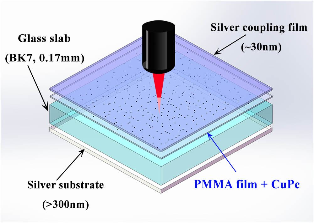
Let us begin with the MCOW structure for Raman detection, which is composed of three parts, as shown in Fig. 1. A thin BK7 glass slab (0.17 mm) and polymethyl methacrylate (PMMA) film containing copper phthalocyanine (CuPc) molecules form the guiding layer, which is sandwiched between two metal films. An thin silver film is deposited on the top of the guiding layer to enable better coupling, whilst another relatively thick film () is deposited at the bottom to prevent light leakage.
Sign up for Chinese Optics Letters TOC. Get the latest issue of Chinese Optics Letters delivered right to you!Sign up now

Figure 1.Schematic diagram of the MCOW structure.
Except for the transverse magnetic () mode[27], the effective refractive index of other guided modes can approach zero, which facilitates direct coupling via the free space coupling technique[28]. The whole structure is similar to an FP resonant cavity, except that the complex refractive index of metal leads to some new features. The manufacture of the waveguide chip is easy, and the sample for detection is added in the PMMA film, whose thickness can be adjusted to modulate the Raman scattering behavior. The purpose of adding a millimeter thick glass slab is twofold: first, polarization independence enables equally efficient coupling for both polarizations; second, the mode density is increased for a thicker guiding layer, which helps to increase the energy coupling efficiency of the focused laser beam.
The physics behind the ultrahigh order modes has been explored in great detail in our previous work[27,29,30]; here, we only include some important facts. The excitation of ultrahigh order modes at a small incident angle manifests itself as a series of resonance dips, which can be observed via monitoring the attenuated total reflection (ATR) spectra of a well collimated laser beam. Figure 2 plots the ATR spectra of both transverse electric (TE) and TM polarization based on Fresnel formulas. The thickness of the coupling layer, silver substrate, PMMA film, and glass slab is set as 30 nm, 300 nm, 7 μm, and 0.17 mm, respectively. Numerical simulation shows the theoretical estimate of the Q factor () of this structure is about . There are nine modes located in the interval from 5° to 15° in Fig. 2, and the reflection spectra of the TE and TM polarizations are overlapped. This is due to the polarization independence of the MCOW, and it proves that this structure is capable of accommodating multiple modes simultaneously if a focused laser beam is applied instead. As mentioned above, the high mode density and the polarization independence are the two key features to achieve high coupling efficiency, which are also the reason for the application of the thick glass slab and the focused laser illumination. The advantage to exciting multiple modes simultaneously can be explained as follows: a single mode exists in the form of an oscillating standing wave in the guiding layer, so the amplitude of the electric field at some parts in the guiding layer is zero. But, if different modes with different periods are excited, no such areas exist in the guiding layer, and together they provide a much more even total electric field distribution. This will facilitate the light–matter interaction and result in stable performance. So, it seems physically practical to enhance the Raman scattering via this waveguide structure; but, now, we address the modulation of Raman scattering efficiency with variable PMMA film thickness.
Figure 2.(Color online) ATR spectra of TE and TM polarization of an MCOW chip. The wavelength is 785 nm, and the dielectric constant of silver, PMMA, and glass is taken as , , and , respectively.
The only adjustable parameter left is the thickness of the PMMA film. We used COMSOL Multiphysics software to calculate the electric field distribution of the single mode in PMMA films of different thicknesses, as shown in Fig. 3. The incident light power is for the two-dimensional (2D) model, and the dielectric constant is same as Fig. 2. For the sake of clarity, the glass slab thickness is set 5 μm, and the PMMA film thickness varies between 0.5 and 1.5 μm, which is sufficient to illustrate the physics behind it. It is obvious that the oscillating fields cover the whole guiding layer at resonance, and whole field intensity is enhanced in comparison with the incident field. The mode density and intensity varies little as the PMMA thickness changes, the only difference is that the thicker PMMA film can support ultrahigh order modes with more nodes, which is illustrated in Fig. 3. In order to illustrate the relation between the Raman enhancement and the light–matter interaction length, we varied the thickness of the PMMA film, while we kept other experimental conditions unchanged. Experiments were carried out to verify the effective modulation of Raman scattering by adjusting the PMMA film thickness, i.e., the interaction length.
Figure 3.Electric field distribution of a single mode in different thicknesses of PMMA films. (a) 0.5, (b) 0.8, (c) 1.0, (d) 1.3, and (e) 1.5 μm.
Raman scattering experiments were carried out to verify the above hypothesis. CuPc was chosen to act as probe molecules due to its excellent properties in optics and chemistry, such as thermostability. To achieve the different spinning thickness of PMMA film, we adopted different concentrations of PMMA solution of trichloromethane (). In the experiment, the PMMA particles of 0.1, 0.4, 0.7, 1.0, and 1.2 g were added in 30 mL , respectively. Then, 0.01 g CuPc was added in each PMMA solution as probe molecules. The CuPc and were purchased from Sinopharm chemical reagent Co. Ltd. The above mixtures were all ultrasonically dissolved. Then, a 200 μL volume of mixed solution was dropped on the center of a glass slab (BK7, ) and span at and . The corresponding thicknesses of the dried layer are 7, 11, 16, 19, and 23 μm, respectively, which are measured via the ellipsometer. So, in preparation of the PMMA film, we kept all the experimental conditions the same except the concentration of the PMMA particles, which results in different film thicknesses. Finally, two silver coatings were deposited on both sides by magnetron sputtering and vacuum evaporation to form the MCOW structure.
For the reflection spectrum of the waveguide, a 100 mW collimated light beam emitted from a single longitudinal mode laser at a wavelength of 785 nm (LBX-785S-100-CIR-PP, Oxxius Co., France) was applied. After passing through a 2 mm diameter aperture and a polarizer [Fig. 4(a)], the laser beam was incident upon the waveguide surface, while a photodiode was used to measure its reflection. A personal computer (PC) controlled goniometer was adopted to carry out angle scanning. Figure 4(b) shows that the intensity of the reflected light varies with the incident angle and forms a series of sharp resonance dips. The experimental result confirms the excitation of the ultrahigh order modes, whilst the deformation from the theoretical simulation in Fig. 2 is due to the absorption, the nonparallelism of the structure, and the divergence of the laser beam. By adjusting the polarizer, the waveguide chip is indeed polarization independent.
Figure 4.(a) Experimental setup for reflectivity detection; (b) the reflection spectra of the MCOW chip with 7 μm PMMA film.
To illustrate the Raman spectra enhancement and the modulation mechanism, a near-infrared Raman spectrometer (Advantage NIRTM, Deltanu) with an excitation wavelength of 785 nm was utilized to collect the scattered light. The probe with a 1.5 cm focal length can focus the excitation light onto the surface of the waveguide vertically. The integration time was 6 s, and the resolution was . The Raman spectra of CuPc in five different thickness waveguides are shown in Fig. 5.
Figure 5.Raman spectra of CuPc obtained via MCOW with five different PMMA film thicknesses: 7, 11, 16, 19, and 23 μm, respectively.
For thicker PMMA films, the Raman spectra intensity is obviously higher. Since the mode intensity and density vary little for the small change in the PMMA film thickness, the physics can only be explained by the increase in the interaction length, which is proportional to the thickness of the PMMA film. Table 1 lists the details of the Raman spectra intensity of CuPc. At least 10 times Raman signal enhancement can be achieved by just modulation of the guiding layer thickness in the MCOW chip. It should be noted that the adjustment of the Raman intensity is through varying the PMMA film thickness in the production process of the waveguide chip in this work. If we use a liquid sample layer instead of the PMMA layer, it is possible to achieve real-time modulation.
| The Intensity Variations of Characteristic Peak Versus the Thickness of PMMA Film |
|---|
| d/μm | 1345 cm−1/a.u. | 1466 cm−1/a.u. | 1558 cm−1/a.u. |
|---|
| 7 | 565 | 213 | 729 |
| 11 | 936 | 295 | 1070 |
| 16 | 1638 | 594 | 2464 |
| 19 | 4185 | 1331 | 5962 |
| 23 | 6661 | 2281 | 9477 |
Table 1. Characteristic Peak Intensity of CuPc in Different Thickness PMMA Films
In conclusion, different from the SERS or the evanescent-field-based Raman spectroscopy, we apply the MCOW structure to enhance Raman signals by exciting the oscillating modes of both TE and TM polarizations. Besides polarization independence, the millimeter scale guiding layer also helps to increase the mode density. Meanwhile, the thickness of the PMMA layer is adjustable during the production process of the waveguide chip, so this can be applied to adjust the Raman intensity, which relies crucially on the interaction volume. Numerical simulation and experimental results confirm that the Raman intensity is enhanced and can be modulated effectively by using this structure. The proposed technique provides a new approach for precise spectroscopy intensity modulation and may facilitate its application in areas such as new optoelectronic devices and lab on a chip in the near future.
References
[1] M. Fleischmann, P. J. Hendra, A. J. Mcquillan. Chem. Phys. Lett., 26, 163(1974).
[2] S. Nie, S. R. Emory. Science, 275, 1102(1997).
[3] K. Kneipp, Y. Wang, H. Kneipp, L. T. Perelman, I. Itzkan, R. R. Dasari, M. S. Feld. Phys. Rev. Lett., 78, 1667(1997).
[4] S. Yampolsky, D. A. Fishman, S. Dey, E. Hulkko, M. Banik, E. O. Potma, V. A. Apkarian. Nat. Photon., 8, 650(2014).
[5] H. Zeng, I. Tai, S. Feng, W. Wang. Biomed. Opt. Express, 6, 3494(2015).
[6] D. Lin, H. Huang, S. Qiu, S. Feng, G. Chen, R. Chen. Opt. Express, 24, 2222(2016).
[7] K. Egodage, C. Matthäus, S. Dochow, I. W. Schie, C. Härdtner, I. Hilgendorf, J. Popp. Chin. Opt. Lett., 15, 090008(2017).
[8] K. Yang, Y. Hu, N. Dong, G. Zhu, T. Zhu, N. Jiang. Biosens. Bioelectron., 94, 286(2017).
[9] L. Liang, H. Qu, B. Zhang, J. Zhang, R. Deng, Y. Shen, S. Xu, C. Liang, W. Xu. Biosens. Bioelectron., 94, 148(2017).
[10] Y. Zheng, X. Zhu, Z. Wang, Z. Hou, F. Gao, R. Nie, X. Cui, J. She, B. Peng. Chin. Opt. Lett., 15, 083001(2017).
[11] L. T. Q. Ngan, K. N. Minh, D. T. Cao, T. A. Cao, V. V. Le. J. Electron. Mater., 46, 3770(2017).
[12] X. Yang, Y. He, X. Wang, R. Yuan. Appl. Surf. Sci., 416, 581(2017).
[13] Z. Xie, Y. Wang, Y. Chen, X. Xu, Z. Jin, Y. Ding, N. Yang, F. Wu. Food Chem., 230, 547(2017).
[14] F. B. Arango, A. Kwadrin, A. F. Koenderink. ACS Nano, 6, 10156(2012).
[15] M. Banik, A. Nag, P. Z. El-Khoury, A. Rodriguez Perez, N. Guarrotxena, G. C. Bazan, V. A. Apkarian. J. Phys. Chem. C, 116, 10415(2012).
[16] M. Moskovits. Phys. Chem. Chem. Phys., 15, 5301(2013).
[17] J. A. Calkins, A. C. Peacock, P. J. Sazio, D. L. Allara, J. V. Badding. Langmuir, 27, 630(2011).
[18] K. J. McKee, M. W. Meyer, E. A. Smith. Anal. Chem., 84, 9049(2012).
[19] Y. Liu, S. Xu, X. Xuan, B. Zhao, W. Xu. J. Phys. Chem. Lett., 2, 2218(2011).
[20] Y. Gu, S. Xu, H. Li, S. Wang, M. Cong, J. R. Lombardi, W. Xu. J. Phys. Chem. Lett., 4, 3153(2013).
[21] K. A. Willets, R. P. Van Duyne. Annu. Rev. Phys. Chem., 58, 267(2007).
[22] D.-B. Hu, Z.-M. Qi. J. Phys. Chem. C, 117, 16175(2013).
[23] Y. Wang, M. Huang, X. Guan, Z. Cao, F. Chen, X. Wang. Opt. Express, 21, 31130(2013).
[24] F. Chen, Z. Cao, Q. Shen, X. Deng, B. Duan, W. Yuan, M. Sang, S. Wang. Appl. Phys. Lett., 88, 161111(2006).
[25] X. Wang, C. Yin, J. Sun, H. Li, Y. Wang, M. Ran, Z. Cao. Opt. Express, 21, 13380(2013).
[26] T. Xu, C. Yin, X. Kan, T. He, Q. Han, Z. Cao, X. Chen. Opt. Lett., 42, 2960(2017).
[27] Z. Cao. Waveguide Optics(2007).
[28] H. Li, Z. Cao, H. Lu, Q. Shen. Appl. Phys. Lett., 83, 2757(2003).
[29] W. Yuan, C. Yin, H. Li, P. Xiao, Z. Cao. J. Opt. Soc. Am. B, 28, 968(2011).
[30] X. Wang, C. Yin, Z. Cao. Progress in Planar Optical Waveguides(2016).