Abstract
The nitrogen vacancy (NV) center in diamond has been well applied in quantum sensing of electromagnetic field and temperature, where the sensitivity can be enhanced by the number of NV centers. Here, we used electron beam irradiation to increase the generation rate of NV centers by nearly 22 times. We systematically studied the optical and electronic properties of the NV center as a function of an electron irradiation dose, where the detection sensitivity of magnetic fields was improved. With such samples with dense NV centers, a sub-pico-Tesla sensitivity in magnetic fields detection can be achieved with optimal controls and detections.The nitrogen vacancy (NV) center in diamond has attracted great interests in the scientific community due to its quantum optical[1–6] and spin properties[7–11]. Most applications in quantum sensing tend to use higher concentrations of ensemble NV center because of their stronger fluorescence emission and higher signal-to-noise ratio[12–14] than single NV centers. The measured sensitivity is then proportional to [15,16], where N is the number of NV centers. In an idealized case in which all other parameters are held constant, increasing the conversion efficiency of NV centers in a fixed detection volume will result in enhanced sensitivity in two ways: first, by increasing the NV center concentration and thus the number of collected photons from the NV center ensemble; and second, by decreasing the concentration of the associated background fluorescence, which improves measurement contrast.
The conversion efficiency of the NV center in diamond depends on the presence of nitrogen atoms and vacancies in the crystal lattice. High-energy particle irradiation, such as electrons, protons, neutrons, or ions, can create vacancies in the crystal[17,18]. In this process, the high-energy particle beam interacts with the crystal and has a certain probability of replacing the carbon atoms in the crystal lattice, leaving a vacancy. The diamond is then annealed at 800°C to diffuse the vacancies in the crystal lattice[19] to recombine with the nitrogen atoms already in the diamond. The final NV center concentration depends on the concentration of the substituted nitrogen as well as the irradiation and annealing parameters[20]. The upper limit of NV center production efficiency is limited by the number of vacancies formed after electron beam irradiation without increasing the nitrogen content of the diamond sample[21].
Here, we used electron beam irradiation to enhance the density of NV centers in diamond. We used a diamond sample with a nitrogen content of 5 ppm (parts per million). After different doses of electron beam irradiation and annealing, the fluorescence saturation curve, spectrum, and spin-related properties were measured. The generation efficiency of the NV center was enhanced by nearly 22 times, and the sensitivity of the magnetic field detection was also improved.
Sign up for Chinese Optics Letters TOC. Get the latest issue of Chinese Optics Letters delivered right to you!Sign up now
The samples used in this study are a chemical vapor deposition (CVD) grown diamond, which was grown on type Ib commercial high-pressure high-temperature (HPHT) (100) oriented single crystal diamond of approximate dimensions from Element-6. Before we used the diamond substrates, they were cleaned in a mixture of sulfuric and nitric acid (1:2) for 1 h at 200°C and by ultrasonic with deionized water, acetone, and isopropanol. Prior to growth, the diamond substrates were pre-treated using a plasma in order to prepare their surfaces for single crystal diamond growth. The microwave plasma CVD system (MPCVD, Seki Technotron Corp., AX-5250S) was used to grow the samples with the microwave power of at a pressure of . The growth temperature was about . Hydrogen (5N), 6% (5N), and a small (about 100 ppm in total gas) addition of nitrogen () were used. The growth time for the sample was 48 h, and the growth rate was about 30 µm/h. After growth, the sample was separated from the HPHT diamond substrate by laser cutting, and both sides of the growth plates were polished by a mechanical polisher. The electron beam injection equipment we used is an electron linear accelerator at Shanghai Gaoying Electronic Technology Co., Ltd. The machine model is DZ-10/20, with the electron beam energy of 10 MeV. The maximum power is 20 kW with energy instability of 1.2%. The pulse beam intensity is 300 mA with the pulse width of 14 µs and the pulse frequency of 452 Hz.
We selected six of the diamond samples generated in the same batch for testing. One of the samples did not undergo electron beam injection. The other five samples were irradiated with the same energy and different doses of electron beams on one side. The energy of the electron beam was 10 MeV. The minimum dose of electron beam irradiation was , and the electron beam irradiation of other samples was twice, four times, eight times, and sixteen times the minimum dose, respectively. All six samples need to be annealed and cleaned in sequence. The vacuum annealing time was 4 h and the annealing temperature and pressure were 800°C and , respectively. After annealing at high temperature, we first cleaned the sample with acetone and ethanol. Then, the sample was rinsed with deionized water to remove the ethanol and dried with nitrogen gas. After that, we used a mixture of 5 mL of perchloric acid, nitric acid, and sulfuric acid to prepare a mixed acid solution for pickling the sample. After the acid solution was ready, the sample was placed therein and heated to 180°C for 2 h.
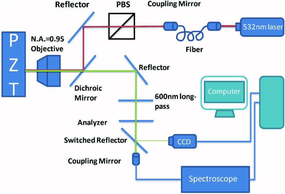
We first tested the six samples by measuring the photo luminance (PL) counts with a homebuilt confocal system, as shown in Fig. 1. During the increase in laser power from 0 to 40 mW, the PL counts collected from each sample increased, as shown in Fig. 2. In the case of the same laser intensity, larger doses of electron beam irradiation will induce more of the generated NV centers and stronger PL intensity. The PL counts with different pump laser power () can be fitted with a saturation function as , where and are saturation counts and pump intensity, respectively. describes the linear dependence of the background from the pump power. From the saturation counts shown in Table 1, we found that the density of the NV center is enhanced by 21.49.

Figure 1.Magnetic sensing system.
Figure 2.PL saturation curves under different electron beam irradiation doses.
| Electron Dose (×1016 cm−2) | Isat(×108 s−1) | α | Enhancement |
|---|
| 0 | 2.07(0.07) | 0.03(1) | 1.00 |
| 1 | 2.94(0.15) | 0.11(1) | 1.42 |
| 2 | 8.44(0.51) | 0.21(1) | 4.01 |
| 4 | 18.30(1.43) | 0.46(2) | 8.84 |
| 8 | 38.06(2.18) | 0.80(4) | 18.39 |
| 16 | 44.49(3.77) | 0.99(6) | 21.49 |
Table 1. PL Saturations of Different Samples
To specifically understand the difference between the PL counts produced by different electron beam irradiation doses at the same laser power, we plotted PL counts versus irradiation doses, as shown in Fig. 3. We found that the four points in the middle of the figure have good linearity. It proved that the dose of the electron beam irradiation is proportional to the number of NV centers within a certain dose of electron beam irradiation. However, after exceeding this range, the PL count tends to be saturated because no nitrogen atoms are introduced during electron beam irradiation. So, the amount of the NV center finally generated is limited by the amount of the original nitrogen atoms inside the material.
Figure 3.PL counts with different electron beam irradiation doses and excitation intensities.
In Fig. 4, we show the spectrum of the fluorescence emission of three samples irradiated by high doses of electron beams. We can obviously see the zero phonon line at 575 nm for the NV center and the phonon sideband at around 680 nm. It is consistent with the growth magnification of Figs. 2 and 3. It shows that after the electron beam irradiation, the NV color center inside the diamond is significantly improved, but it cannot be improved by the internal nitrogen content.
Figure 4.Spectra of NV color centers with different electron beam irradiation doses.
The NV center is an ideal sensor for quantum sensing[22] of weak magnetic fields. Some important spin parameters affect the sensitivity[23] of the final magnetic field measurement, such as , , and . In the experiment, we first used the laser to prepare the NV center to state , and then added a microwave pulse to change the color center to a superposition state . After a period of time without any microwave or optical operation, the system will become mixed due to environmental noise, which is called free induction decay (FID) time. Due to the effect of noise, the image we observe in the non-resonant case is a trigonometric oscillation linearity of an exponential envelope. The characteristic time of this exponential function is . In order to eliminate the influence of the noisy magnetic field, we divide the FID time into two segments by adding a pulse in the middle of the two pulses to make the spin echo measurement. The depolarization dynamics of the NV center ensemble is characterized by measurement. The data are shown in Table 2. It can be seen from the data that as the electron beam irradiation dose increases, the changes in , , and are not obvious. It can be seen that the electronic spin properties of NV centers have not changed greatly due to the injection of electrons.
| Electron Dose (×1016 cm−2) | T2* (ns) | T2 (μs) | T1 (ms) |
|---|
| 0 | — | 80(4) | — |
| 1 | 310(20) | 75(2) | 2.6(2) |
| 2 | 458(21) | 73(2) | 2.5(2) |
| 4 | 313(53) | 125(5) | 3.7(4) |
| 8 | 447(23) | 79(3) | 3.5(3) |
| 16 | 377(60) | 77(4) | 2.3(4) |
Table 2. Decoherence Times for Different Samples
Besides the decoherence times, the contrast () of the optically detected magnetic resonance (ODMR) is also the key parameter to determine the sensitivity of the magnetic field measurement with NV centers. We measured the ODMR contrasts of these samples, as shown in Fig. 5. With the decoherence times and the contrast of ODMR, the sensitivity[23] for DC and AC magnetic field measurement with NV centers can be and with , where is the number of photons collected per measurement. The sensitivities with different samples are listed in Table 3. As can be seen from the data in Table 3, the sensitivity of the NV-center-based magnetic field measurement does not change much as the injected electron dose increases. In an alternating magnetic field, the minimum sensitivity is one-third of the start. The main reason is that the contrast of ODMR decreases so much because of the spectrum inhomogeneous broadening in such samples with dense NV centers. It can be further overcome by time-gated fluorescence detection control[24] and spin state control with composite pulses[25].
Figure 5.ODMR contrast of the samples with different electron beam irradiation doses.
| Electron Dose (×1016 cm−2) | C(%) | n | ηdc(nT/Hz1/2) | ηac(nT/Hz1/2) |
|---|
| 0 | 4.7(1) | 49.7(2.5) | — | 7.59(36) |
| 1 | 5.5(1) | 94.8(4.7) | 38.12(1.91) | 3.85(16) |
| 2 | 4.5(1) | 229.8(11.5) | 24.61(1.13) | 3.06(12) |
| 4 | 3.3(2) | 402.9(20.1) | 30.67(2.85) | 2.41(14) |
| 8 | 2.8(1) | 822.2(41.1) | 21.18(1.02) | 2.50(14) |
| 16 | 1.6(1) | 929.9(46.5) | 38.67(3.09) | 4.25(27) |
Table 3. Magnetic Field Measurement Sensitivity for DC and AC Magnetic Fields
In the process of electron beam irradiation of the sample, we used single-sided irradiation. To understand whether the irradiation process has an effect on the diamond surface lattice, we used an X-ray diffraction (XRD) instrument to detect the damage to the diamond surface lattice and changes in the single crystal. Here, we refer to the side of the sample, which is directly irradiated by the electron beam, as the front side and the other side as the back side. When the electron beam injection dose exceeds , the side peak in XRD would appear in the experiment. As shown in Fig. 6(a), we found that on the front side, in addition to the main peak of 120°, there is a small peak of about 51.16° with a very weak intensity. We estimated that was from the stray peaks caused by the damage of the diamond surface lattice. In the back side, there is no such small peak. The rocking curves in XRD on both sides are shown in Fig. 6(b). We found that the full width at half-maximum of the front side is significantly larger than that on the back side, so that the monocrystalline of the front side is different from the other side. It can be seen that electron beam irradiation has done some damage to the single crystal of the sample surface.
Figure 6.(a) XRD intensity of front side and (b) XRD rocking curves on both sides.
In conclusion, we systematically studied the optical and electronic properties of the NV center and material damage in synthetic diamonds, as a function of the electron irradiation dose. When the dose of electron beam irradiation is small, the fluorescence intensity increases linearly with the irradiation dose. When the electron beam irradiation dose is large, the fluorescence growth is slowed down by the amount of nitrogen atoms in the material. It shows that electron beam irradiation can greatly increase the generation rate of the NV center in diamond. We observed that the , , and are basically not changed much. We found that the contrast of the ODMR decreases significantly as the electron beam irradiation dose increases, which mainly induces the weak improvement in the detection sensitivity of the magnetic field. However, by combining with the time-gated fluorescence detection control[24] and spin state control with composite pulses[25], we hope to get a sub-pico-Tesla (pT) sensitivity with such samples with dense NV centers.
References
[1] I. Aharonovich, A. D. Greentree, S. Prawer. Nat. Photon., 5, 397(2011).
[2] S.-J. Peng, Y. Liu, W.-C. Ma, F.-Z. Shi, J.-F. Du. Acta Phys. Sin., 67, 167601(2018).
[3] M. Chen, C. Meng, Q. Zhang, C.-K. Duan, F.-Z. Shi, J.-F. Du. Natl. Sci. Rev., 5, 346(2017).
[4] Y. Dong, B. Du, S.-C. Zhang, X.-D. Chen, F.-W. Sun. Acta Phys. Sin., 67, 160301(2018).
[5] G.-Q. Liu, J. Xing, X.-Y. Pan. Acta Phys. Sin., 67, 120302(2018).
[6] C.-C. Li, X.-D. Chen, S. Li, F.-W. Sun. Chin. Opt. Lett., 14, 072701(2016).
[7] W.-H. He, M.-M. Dong, Z.-Z. Hu, Q.-H. Zhang, B. Yang, Y. Liu, X.-L. Fan, G.-X. Du. Chin. Phys. Lett., 36, 127601(2019).
[8] C. Zhang, H. Yuan, N. Zhang, L. Xu, J. Zhang, B. Li, J. Fang. J. Phys. D., 51, 155102(2018).
[9] L.-M. Zhou, Y. Dong, F.-W. Sun. Chin. Phys. Lett., 32, 067601(2015).
[10] Y. Dong, Y. Zheng, S. Li, C. C. Li, X. D. Chen, G. C. Guo, F. W. Sun. Npj Quantum Inform., 4, 3(2018).
[11] Y. Dong, X.-D. Chen, G.-C. Guo, F.-W. Sun. Phys. Rev. A, 94, 052322(2016).
[12] T. Wolf, P. Neumann, K. Nakamura, H. Sumiya, T. Ohshima, J. Isoya, J. Wrachtrup. Phys. Rev. X, 5, 041001(2015).
[13] M. Chipaux, A. Tallaire, J. Achard, S. Pezzagna, J. Meijer, V. Jacques, J.-F. Roch, T. Debuisschert. Eur. Phys. J. D, 69, 166(2015).
[14] D. R. Glenn, D. B. Bucher, J. Lee, M. D. Lukin, H. Park, R. L. Walsworth. Nature, 555, 351(2018).
[15] S. F. Huelga, C. Macchiavello, T. Pellizzari, A. K. Ekert, M. B. Plenio, J. I. Cirac. Phys. Rev. Lett., 79, 3865(1997).
[16] D. Budker, M. Romalis. Nat. Phys., 3, 227(2007).
[17] I. Aharonovich, C. Santori, B. A. Fairchild, J. Orwa, K. Ganesan, K.-M. C. Fu, R. G. Beausoleil, A. D. Greentree, S. Prawer. J. Appl. Phys., 106, 124904(2009).
[18] J. Havlik, V. Petrakova, J. Kucka, H. Raabova, D. Panek, V. Stepan, Z. Zlamalova Cilova, P. Reineck, J. Stursa, J. Kucera, M. Hruby, P. Cigler. Nat. Commun., 9, 4467(2018).
[19] K. Iakoubovskii, I. Kiflawi, K. Johnston, A. Collins, G. Davies, A. Stesmans. Phys. B Condens. Matter, 340, 67(2003).
[20] F. Waldermann, P. Olivero, J. Nunn, K. Surmacz, Z. Wang, D. Jaksch, R. Taylor, I. Walmsley, M. Draganski, P. Reichart, A. Greentree, D. Jamieson, S. Prawer. Diam. Relat. Mater., 16, 1887(2007).
[21] J. Botsoa, T. Sauvage, M.-P. Adam, P. Desgardin, E. Leoni, B. Courtois, F. Treussart, M.-F. Barthe. Phys. Rev. B, 84, 125209(2011).
[22] Y. Zheng, F.-W. Sun. Chin. Opt. Lett., 17, 060901(2019).
[23] C.-H. Li, Y. Dong, J.-Y. Xu, D.-F. Li, X.-D. Chen, A.-M. Du, Y.-S. Ge, G.-C. Guo, F.-W. Sun. Appl. Phys. Lett., 113, 072401(2018).
[24] X.-D. Chen, Y. Zheng, B. Du, D.-F. Li, S. Li, Y. Dong, G.-C. Guo, F.-W. Sun. Phys. Rev. Appl., 11, 064024(2019).
[25] J.-Y. Xu, Y. Dong, S.-C. Zhang, Y. Zheng, X.-D. Chen, W. Zhu, G.-Z. Wang, G.-C. Guo, F.-W. Sun(2018).