• Chinese Physics B
  • Vol. 29, Issue 9, (2020)
Xiang Wang1、2, Chen Ge1、2、†, Ge Li1, Er-Jia Guo1, Meng He1, Can Wang1、2、3, Guo-Zhen Yang1, and Kui-Juan Jin1、2、3
Author Affiliations
  • 1Institute of Physics, Chinese Academy of Sciences, Beijing 0090, China
  • 2University of Chinese Academy of Sciences, Beijing 100049, China
  • 3Songshan Lake Materials Laboratory, Dongguan 52808, China
  • show less
    DOI: 10.1088/1674-1056/aba60c Cite this Article
    Xiang Wang, Chen Ge, Ge Li, Er-Jia Guo, Meng He, Can Wang, Guo-Zhen Yang, Kui-Juan Jin. A synaptic transistor with NdNiO3[J]. Chinese Physics B, 2020, 29(9): Copy Citation Text show less
    The structure and property of electrolyte gated NdNiO3 transistor. (a) The crystal structure of NdNiO3 film grown on LaAlO3 substrate. (b) The R–T measurements for different thickness NdNiO3 films on LaAlO3 substrates. (c) Schematic diagram of the electrolyte-gated transistor. (d) The transfer curve. The source–drain current ID and the gate current IG are shown as a function of the gate voltage. Arrows indicate the gate bias sweeping direction.
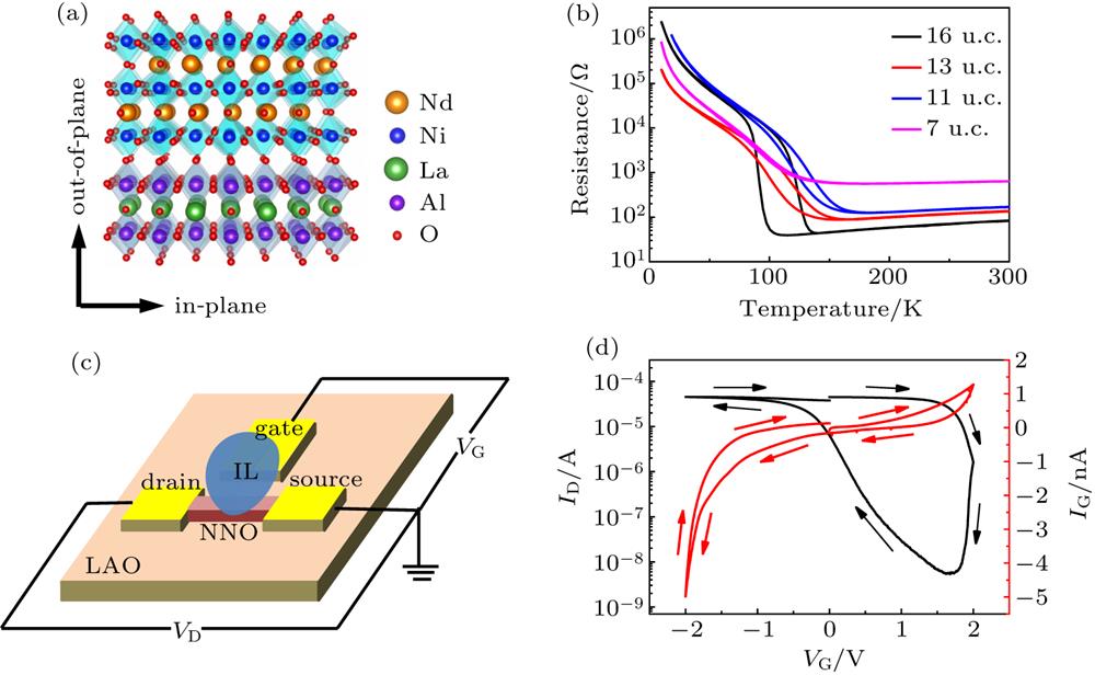
    Fig. 1. The structure and property of electrolyte gated NdNiO3 transistor. (a) The crystal structure of NdNiO3 film grown on LaAlO3 substrate. (b) The RT measurements for different thickness NdNiO3 films on LaAlO3 substrates. (c) Schematic diagram of the electrolyte-gated transistor. (d) The transfer curve. The source–drain current ID and the gate current IG are shown as a function of the gate voltage. Arrows indicate the gate bias sweeping direction.
    The dependence of the channel current on the gate spikes. (a) The same spike time (0.4 s) with different spike voltages. (b) The source–drain current ID of (a) intercepted from 40 s is shown as a function of gate voltage. (c) The same spike voltage (+1.4 V) with different spike time. (d) The source–drain current ID of (c) intercepted from 40 s is shown as a function of spike time. Here, the VD was 5 mV.
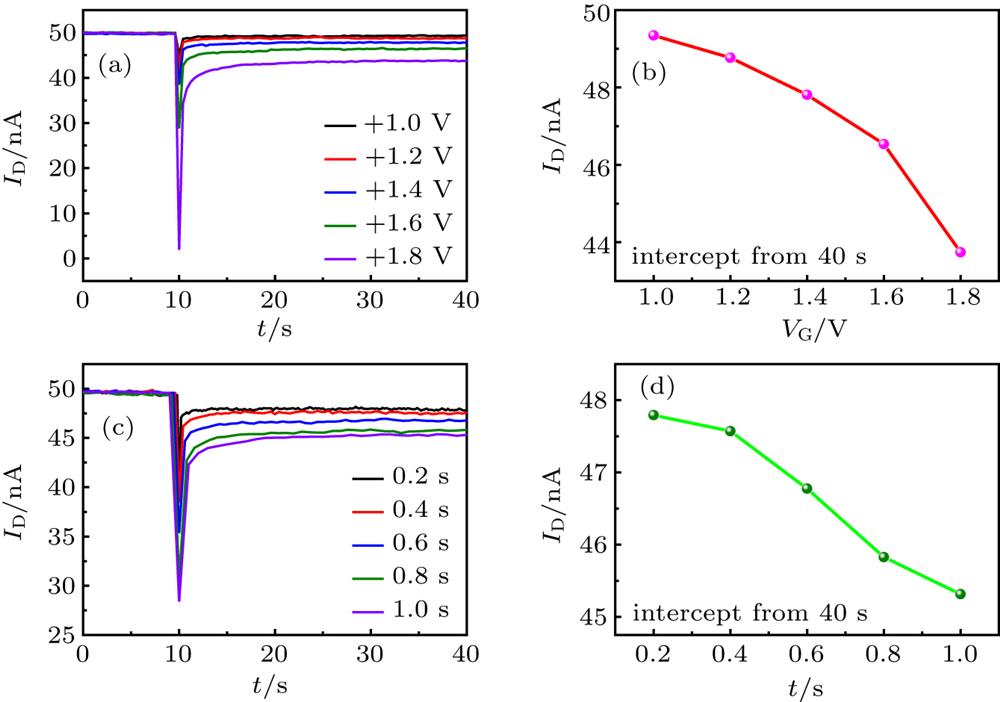
    Fig. 2. The dependence of the channel current on the gate spikes. (a) The same spike time (0.4 s) with different spike voltages. (b) The source–drain current ID of (a) intercepted from 40 s is shown as a function of gate voltage. (c) The same spike voltage (+1.4 V) with different spike time. (d) The source–drain current ID of (c) intercepted from 40 s is shown as a function of spike time. Here, the VD was 5 mV.
    The conductance modulation of NdNiO3 transistor. (a) The channel conductance changes with pulse groups. Firstly, the positive gate voltage +1.8 V with pulse width 200 ms was applied, and the pulse number is 5, 10, 15, 20, respectively. Then, the negative gate voltage −1.6 V sequence was applied, and the pulse number is 20, 15, 10, 5, respectively. All the pulse groups were spaced about 180 s. (b) Repeatability of long-term synaptic potentiation and depression.
    Fig. 3. The conductance modulation of NdNiO3 transistor. (a) The channel conductance changes with pulse groups. Firstly, the positive gate voltage +1.8 V with pulse width 200 ms was applied, and the pulse number is 5, 10, 15, 20, respectively. Then, the negative gate voltage −1.6 V sequence was applied, and the pulse number is 20, 15, 10, 5, respectively. All the pulse groups were spaced about 180 s. (b) Repeatability of long-term synaptic potentiation and depression.
    STDP characteristics of NdNiO3 transistor device. The applied pre- and post-spikes for the (a) asymmetric and (b) symmetric STDP functions. (c) Asymmetric and (d) symmetric STDP implemented in the NdNiO3 electrolyte-gated synaptic transistors.
    Fig. 4. STDP characteristics of NdNiO3 transistor device. The applied pre- and post-spikes for the (a) asymmetric and (b) symmetric STDP functions. (c) Asymmetric and (d) symmetric STDP implemented in the NdNiO3 electrolyte-gated synaptic transistors.
    Xiang Wang, Chen Ge, Ge Li, Er-Jia Guo, Meng He, Can Wang, Guo-Zhen Yang, Kui-Juan Jin. A synaptic transistor with NdNiO3[J]. Chinese Physics B, 2020, 29(9):
    Download Citation