
Ge Yaqiong, Chen Xing, Chang Zexin. Crystallization Behavior of Zr-Based Amorphous Alloy Prepared by Selective Laser Melting[J]. Chinese Journal of Lasers, 2020, 47(12): 1202002
- Chinese Journal of Lasers
- Vol. 47, Issue 12, 1202002 (2020)
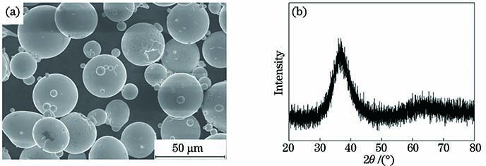
Fig. 1. SEM image and XRD pattern of Zr50 amorphous alloy powders. (a) SEM image; (b) XRD pattern
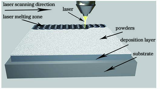
Fig. 2. Diagram of selective laser melting
Fig. 3. Macroscopic appearance and XRD pattern of Zr50 amorphous alloy prepared by selective laser melting. (a) Macroscopic appearance; (b) XRD pattern
Fig. 4. Microstructures of cross-section of Zr50 amorphous alloy formed by selective laser melting. (a) Upper part of deposition layer; (b) middle part of deposition layer; (c) bottom of deposition layer and its junction with the substrate
Fig. 5. Back scatter images of Zr50 amorphous alloy. (a) Microstructure; (b) partially enlarged area
Fig. 6. TEM images of Zr50 amorphous alloy. (a) Coexistence zone of amorphous zone and crystallization zone; (b) nanocrystalline
Fig. 7. Schematics of weld bead superposition process. (a) Schematic of single weld bead; (b) schematic of weld bead superposition
Fig. 8. Schematics of superposition process of deposition layers. (a) Schematic of multi-weld bead superposition of single-layer deposition layer; (b) schematic of superposition between multi-layer deposition layers
Fig. 9. Thermal cycle curve of superposition area of heat affected zone. (a) Weld bead superposition; (b) deposition layer superposition
Fig. 10. Diagram of selective laser melting preparation process of bulk amorphous alloy
Fig. 11. Thermal cycle curves of Zr50 bulk amorphous alloy prepared by selective laser melting

Set citation alerts for the article
Please enter your email address
© Copyright 2018-2021 | Chinese Laser Press. All Rights Reserved 沪ICP备15018463号-20