 AI Video Guide
  AI Picture Guide
 AI One Sentence

Yuxi Li, Jiafu Wang, Sai Sui, Ruichao Zhu, Yajuan Han, Hongya Chen, Xinmin Fu, Shaojie Wang, Cunqian Feng, Shaobo Qu, "Simplistic framework of single-pixel-programmable metasurfaces integrated with a capsuled LED array," Photonics Res. 12, 884 (2024)
- Photonics Research
- Vol. 12, Issue 5, 884 (2024)
Note: This section is automatically generated by AI . The website and platform operators shall not be liable for any commercial or legal consequences arising from your use of AI generated content on this website. Please be aware of this.
Abstract
1. INTRODUCTION
A metasurface is an artificial material composed of an array of subwavelength structures arranged periodically or quasi-periodically on a two-dimensional surface, which has extraordinary physical properties that natural materials do not have, and its material properties are mainly derived from artificial structures rather than the material components that make up its structure [1–5]. The meta-atom structure produces an “abrupt phase shift” that can modulate electromagnetic (EM) wave without obeying the traditional law of reflection/refraction [1]. Through proper design, the appropriate subwavelength meta-atom structure is determined, to present a gradient distributed phase in the plane direction. Based on this characteristic, the incident EM wave will respond in accordance with the set gradient direction, and its phase, amplitude, polarization state, and other propagation characteristics can be arbitrarily controlled [6–8]. So far, many functional devices based on metasurfaces have been implemented [9], such as planar retroreflectors [10], optically variable devices [11], microwave imagers [12], and optical components [13], which have great application potential. In order to solve the bottleneck imposed by the narrow field of view and large volume of the lens system, a transparent metalens with anisotropic response was fabricated based on the metasurface, which has a large numerical aperture and broadband characteristics [14]. Metasurfaces are applied to the antennas field with unexpected effects. A metasurface antenna based on a small electric resonator was designed to provide beam-steering capabilities by properly phasing all resonators [15]. Metasurfaces can also be used to eliminate chromatic aberration in the continuous wavelength region [16]. At the same time, the metasurface has the advantages of thin thickness, low loss, and simple manufacturing, which has attracted widespread attention [17–20].
However, once these metasurfaces are designed, those functions are settled, and cannot be changed freely. Fortunately, a number of multi-functional metasurfaces have been proposed that have different functions for different polarization waves [21–23]. Loading the active material or PIN diode into the metasurface, the phase of EM wave can modulate through changing the voltage across the meta-atom, which can achieve both dynamic beam steering and reconfigurable beam focusing [24], generate different complex beams such as Bessel beam, vortex beam, and Airy beam [25], and perform beam deflection and polarization transformation [26]. A generative adversarial network can be introduced into the design of the multi-functional metasurface to construct devices with different functions such as a bifocal metalens, polarization multiplexed beam deflector, polarization multiplexed metalens, and polarization independent metalens [27].
With the rapid development of metasurfaces, a coding metasurface based on binary discrete coding is proposed, which combines the physical metasurface with the concept of binary code in the field of information storage and transmission [3]. This pushes the design of the metasurface to a new field. One of the main advantages of coding metasurfaces is that EM properties can be described by finite discrete digital states, which are currently widely used [28]. The coding metasurfaces are used to realize holographic images [29], multi-frequency modulation [30], control the transmission, absorption, and reflection of EM waves [31,32], polarization conversion [33], and wireless communication [34–37]. In order to ensure that the meta-atom has the characteristics of state switching, tunable active devices such as diodes need to be embedded in the unit [30,31,38,39]. It is worth noting that brain signal acquisition technology can be employed in coding metasurfaces. The acquired brain wave signal is converted into a voltage signal of the control diode by an excitation device and multi-electromagnetic functions and wireless communication can be realized. The scattering pattern of EM waves can change dynamically according to the brain waves [40]. In addition, it is possible to integrate additional sensors [41] or embed pre-trained artificial neural networks [42] on the metasurface. Through sensing changes in the external environment, different DC bias voltages are fed to the diode to adaptively adjust the reflection characteristics of the metasurface, and finally realize different EM functions. However, in order to switch the state, most of the controllable metasurfaces are designed based on external excitation devices with the wired electrical control method, which requires a large number of feeders to connect the circuit with the DC power supply and the interface of the metasurface, which will increase the design complexity of the system and bring problems to the control and motion of the digital coding metasurface. Moreover, as the size of the array increases, the size of the feeder network also increases, and its design difficulty also increases.
Sign up for Photonics Research TOC. Get the latest issue of Photonics Research delivered right to you!Sign up now
Therefore, in order to simplify the control of coding metasurfaces, other control methods need to be explored [43]. At present, the light control method is gradually rising, replacing the traditional electronic control method, which has produced unexpected effects. Photoelectric detection circuits are integrated into metasurfaces to detect optical signals. The microwave reflection spectrum is manipulated through using optical signals, which can well generate symmetrical harmonics and white-noise-like spectra [44]. And the optical signal can also be modulated to encode the meta-atom, which generates a specific scattering field and achieves beam deflection [45]. In addition, the varactor diode and photoresistor are integrated to adjust the light source, and the reflection phase is regulated to realize the pencil beam scanning and orbital angular momentum beam at the microwave frequency [46]. Different from the traditional wired electrical control method, the optical control method can provide the drive signal in a non-contact way through light, which has unique advantages such as simplifying the system device and reducing signal cross talk. However, this control method still retains the bias circuit used to control the active device, which is not conducive to large-scale applications, and the existence of the bias circuit also inevitably causes the interference with EM transmission [47]. In order to reduce the influence of bias circuits on EM waves, the metal structure needs to be fully optimized, which inevitably increases the difficulty of metasurface design [48].
Based on the above research status, the simplistic framework of single-pixel-programmable metasurfaces (SPPMs) integrated with a capsuled LED array is proposed to dynamically control EM waves, which is mainly composed of an LED array and metasurface, as shown in Fig. 1. Different from traditional light control methods, the photoresistor as a part is fully embedded in the meta-atom. The luminous intensity of the LED array is controlled by the computer, changing the photoresistor value to modulate the phase response in the framework. The LED array lamp beads and the meta-atoms have one-to-one correspondence to achieve the purpose of single-pixel programming. With this manner, the complex biasing network is removed and transformed to the computer-controlling light source, and thus the functions of the metasurface can be switched by changing the light lattice. This control method suppresses the traditional design method of external excitation devices based on wired electronic control methods, which can reduce the complexity of system design. The lamp bead is placed in the metasurface hole, which is equivalent to being in a confined space, emitting the light source in a non-invasive way, which will not affect other equipment, and at the same time can reduce the interference of the external light source on the photoresistor, with strong anti-interference. The LED array and metasurface are closely combined to achieve a simple integrated design, reducing the space required and more in line with practical applications. More importantly, the influence of additional devices on EM wave transmission can be reduced.
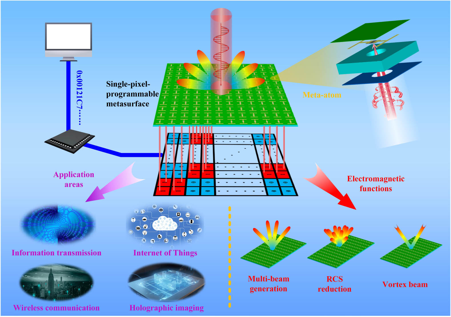
Figure 1.Schematic diagram of the principle of SPPM and its application.
An SPPM embedded in the photoresistors was designed, fabricated, and measured for verification. According to the schematic diagram of Fig. 1, the LED array is encoded according to the coding sequence corresponding to different functions. The lamp bead bright is encoded as “1,” and the lamp bead dark is encoded as “0.” Since the resistance value of the meta-atom is different, the reflected phase is also different. When EM waves are incident to coding metasurfaces, different reflected beams are generated according to different coding sequences to achieve various functions. This work provides a new design idea for massive programmable metasurfaces, which is highly applicable to multiple beam generation, RCS reduction, vortex beam, and other functions by encoding LED arrays. More importantly, it lays a foundation for the development of intelligent control metasurfaces, provides a new direction, and has broad application prospects in the fields of information transmission, mobile communication, wireless coverage blinding, holographic imaging, and adaptive intelligent perception.
2. META-ATOM STRUCTURE DESIGN
A dynamic meta-atom is designed, as shown in Figs. 2(a)–2(c). The meta-atom consists of four layers, the first layer of which is a top film, using PI material (dielectric constant
![]()
Figure 2.Dynamic meta-atom: (a)–(c) structure diagram and geometric parameters; (d) simulated reflection amplitude in the “0,” “1” states; (e) simulated reflection phase in the “0,” “1” states; (f), (g) surface current distribution in the “0,” “1” states.
The period of each meta-atom structure is
3. RESULTS
A. Simulation Results
In this paper, the GT36516 photoresistor is selected as the lossy device of the meta-atom. Through inquiring the technical book, the resistance value can reach 0.3 MΩ in the dark environment. First, the most critical step is to determine the resistance values corresponding to the codes “0” and “1.” Through the utilization of CST Microwave Studio software, the designed meta-atom is simulated and optimized. A large amount of simulation data are obtained through changing the photoresistor value, and the amplitude and phase diagrams under different resistance values are shown in Figs. 6(a) and 6(b), respectively. At the frequency of 7.678 GHz, the reflection phase difference between 100 Ω and 0.3 MΩ is 180°, and the amplitude is relatively close, as shown in Figs. 2(d) and 2(e), which satisfies the condition of phase modulation. See Appendix A for more details on the conditions of meta-atom phase modulation. The meta-atom surface currents in different states are shown in Figs. 2(f) and 2(g), respectively.
Then,
![]()
Figure 3.Simulation diagram: (a)–(c) distribution diagrams of meta-atom state for different coding sequences; (d)–(f) far-field scattering pattern for theory of different coding sequences; (h)–(i) far-field scattering pattern for simulation of different coding sequences.
B. Experimental Results
A sample is fabricated as shown in Fig. 4(a) to verify the SPPM adjustment beam function. The 2835 lamp beads are integrated on the aluminum substrate to make an LED array through the utilization of integrated circuit packaging technology to control the photoresistor value, as shown in Fig. 4(b). The connection diagram of the system device is shown in Fig. 4(c). First, the S-parameters of the experimental sample are measured. In the microwave anechoic room, in order to test the reflection amplitude and phase, the experimental sample and a pair of horn antennas are placed as shown in Fig. 4(d), with one horn antenna as the transmitting antenna and the other horn antenna as the receiving antenna. Through the LED array control system to control the full on and off of the lamp beads, the S-parameters in the “0” and “1” states are measured, as shown in Figs. 5(a) and 5(b). According to the experimental data, it can be obtained that when the frequency is 5.7 GHz, the reflected phase difference is 180°, and the amplitude is relatively close, which meets the conditions of phase modulation. Comparing Figs. 2(d) and 2(e) with Figs. 5(a) and 5(b), it can be observed that there are errors between the simulation data and the experimental data. On the one hand, it may be caused by the generated capacitance or inductance after the photoresistor is integrated, and on the other hand, it may be caused by processing errors that the actual size of the metasurface structure is inconsistent with the ideal simulation parameters. See Appendix D for more details on frequency shift due to parameter errors.
![]()
Figure 4.Diagram of the experiment setup: (a) experimental sample; (b) LED array; (c) device connection diagram; (d) diagram of S-parameter experimental measurement devices; (e) diagram of far-field scattering pattern experimental measurement devices.
![]()
Figure 5.Experimental measurement results: (a), (b) S-parameter measurement results; (c), (d) counterclockwise, clockwise measurement results of four beams; (e) measurement result of RCS reduction; (f) measurement result of vortex beam.
Next, the far-field scattering pattern is tested under different coding sequences and the experimental setup is shown in Fig. 4(e). A pair of horn antennas with an operating frequency of 5.2–8.2 GHz are used, one of which is used as the transmitting antenna, placed on the turntable with the sample and rotates with the sample, and the other horn antenna is placed at the far end as the receiving antenna. At the beginning moment, two horn antennas are facing the processed sample. According to the coding sequence shown in Fig. 3(a), the LED array is adjusted to change the resistance value. According to Figs. 3(d) and 3(g), the simulation results show that the beams are not in the
4. CONCLUSIONS
In summary, we proposed a simplistic framework of SPPMs integrated with capsuled LED array in this paper to dynamically control EM waves, the basic idea of which is to use the computer to convert the coding sequence into hexadecimal frames, which is input to the LED array control board to control the on–off of the LED array lamp beads. This simplistic framework completely embeds the photoresistor as a part of the meta-atom, without a large number of feeders, and realizes the purpose of control in a non-contact manner through the optical signal, which has the advantages of fast response, strong anti-interference, and low design complexity, and can reduce the impact of additional devices on EM wave transmission. Both simulation and experiment results show that the programmable metasurface can generate different reflected beams and customize different far-field scattering patterns, which proves the feasibility and effectiveness of the simplistic framework proposed in this paper to control the metasurface scattering or radiation characteristics. This work enriches the control method of the programmable metasurface and provides a new idea for subsequent research. More importantly, it also lays the foundation for metasurface intelligent perception and adaptive regulation with broad development prospects in many fields such as information communication, Internet of Things, wireless communication, and adaptive intelligent perception.
Acknowledgment
Acknowledgment. The authors are grateful to the support from the National Key Research and Development Program of China, the National Natural Science Foundation of China, and the Natural Science Foundation of Shaanxi Province.
APPENDIX A: CONDITIONS OF META-ATOM PHASE MODULATION
According to Fig.
![]()
Figure 6.Simulation results: (a) amplitude at different resistance values; (b) phase at different resistance values.
APPENDIX B: CALCULATION OF CODING SEQUENCE
According to the generalized Snell’s law for the metasurface,
If the EM wave is incident perpendicular to the metasurface, the reflection angle can be calculated as
Based on the above results, the coding sequence in one direction can be obtained, and in order to generate four beams, the same code needs to be performed in the other direction. Then the two directions are superimposed, and the coding sequence is shown in Fig.
If the reflected phases of the individual meta-atoms are randomly distributed, the metasurface can scatter the energy of the reflected wave, reducing the RCS caused by the metasurface, which can be given by Eq. (
Figure
The reflection phase of the individual meta-atoms on the metasurface is calculated according to the reflection angle
The coding sequence of the vortex beam is calculated according to Eqs. (
APPENDIX C: PHOTORESISTOR PARAMETER TEST
In this paper, 2835 lamp beads with wavelengths of 520 nm, 560 nm, 590 nm, and 620 nm are selected as the light source to measure the photoresistor resistance, and the specific data are shown in Table
Photoresistor Values in Different Situations
| 3 mm | 4 mm | 5 mm | 10 mm | 15 mm | ||
|---|---|---|---|---|---|---|
| 520 nm | Light intensity (lx) | 110,000 | 97,000 | 88,000 | 43,000 | 25,000 |
| Resistance (Ω) | 148 | 153 | 160 | 244 | 297 | |
| 560 nm | Light intensity (lx) | 75,500 | 66,000 | 60,000 | 27,000 | 17,000 |
| Resistance (Ω) | 92 | 102 | 110 | 167 | 216 | |
| 590 nm | Light intensity (lx) | 56,500 | 36,000 | 30,000 | 22,000 | 11,100 |
| Resistance (Ω) | 70 | 82 | 90 | 118 | 180 | |
| 620 nm | Light intensity (lx) | 88,000 | 85,000 | 83,000 | 50,000 | 26,000 |
| Resistance (Ω) | 49 | 56 | 65 | 84 | 113 |
APPENDIX D: THE EFFECT OF PARAMETER ERROR ON THE RESONANT FREQUENCY
S-parameter simulation results under different
![]()
Figure 7.S-parameter simulation results under different structural parameters: (a), (b) S-parameter simulation results under different
![]()
Figure 8.S-parameter simulation results under different device parameters: (a), (b) S-parameter simulation results under different inductances when the capacitance is 0.5 pF; (c), (d) simulation results of S-parameters under different capacitances when the inductance is 0.5 nH.
APPENDIX E: THE PHASE DISTRIBUTION AND THE TWO-DIMENSIONAL FAR-FIELD SCATTERING PATTERN
The phase distribution is shown in Figs.
![]()
Figure 9.Phase distribution and two-dimensional far-field scattering pattern of different EM functions: (a), (b) four beams; (c), (d) RCS reduction; (e), (f) vortex beam.
References
[9] X. G. Zhao, Z. C. Sun, L. Y. Zhang. Review on metasurfaces: an alternative approach to advanced devices and instruments. Adv. Devices Instrum., 2022, 9765089(2022).


Set citation alerts for the article
Please enter your email address

© Copyright 2018-2021 | Chinese Laser Press. All Rights Reserved 沪ICP备15018463号-20