1National Engineering Laboratory for TFT-LCD Technology, Department of Electrical Engineering, Shanghai Jiao Tong University, Shanghai 200240, China
2Key Laboratory for Laser Plasmas (Ministry of Education) and Department of Physics and Astronomy, Shanghai Jiao Tong University, Shanghai 200240, China
3Collaborative Innovation Center of IFSA (CICIFSA), Shanghai Jiao Tong University, Shanghai 200240, China
4Department of Xiamen Institute of Measurement and Testing, Xiamen 361000, China
5State Key Laboratory on Integrated Optoelectronics, Institute of Semiconductors, Chinese Academy of Sciences, Beijing 100083, China
Ping Ma, Xuecheng Cui, Jun Zheng, Pinchun Kang, 志成 叶. Slim OFRS based on a grating input coupler and a microprism sensing surface[J]. Chinese Optics Letters, 2016, 14(11): 112303
Copy Citation Text
A slim optical fingerprint recognition sensor (OFRS) based on a grating input coupler and a microprism sensing surface is proposed. By using a subwavelength grating coupler, input light is coupled into the planar waveguide and the propagation angle is well engineered to avoid image overlap, thus an undistorted fingerprint is captured. For maintaining a thin structure, a microprism array is utilized to facilitate the breaking of total internal reflection under a large diffraction angle from the grating. The feasibility, efficiency, and image quality of the proposed structure are verified and discussed. The device has the advantages of a slim structure, a high image contrast, and a compact architecture, suitable for mobile devices.
Fingerprint recognition technology plays an important role in information security, especially for access controllers and mobile devices. There have been a variety of sensing approaches to capturing fingerprints that have advantages and weaknesses[1]. Capacitive fingerprint sensors[2] are widely used in mobile phones owing to their thin structure, but the cost is rather high because of the small size of the sensing units. Also, the opaqueness of the sensing area brings about more difficulties for the capacitive type to be embedded on a display screen, such as the Apple Touch ID[3], which places the capacitive sensors on the nontransparent “home” button. Although ultrasonic types[4] can capture a 3D fingerprint image with a high image quality, their cost is even higher due to the need for piezoelectric materials. Optical sensors are more attractive in view of the economic concerns as well as their superb durability. As an example of the mature application of an optical fingerprint recognition sensor (OFRS) in an access control system, usually a right angle prism is used to reflect laser beams by total internal reflection (TIR) and then the fingerprints put on the hypotenuse are obtained[5]. However, the bulky prism makes it impossible to be integrated into smart devices. Consequently, several types of OFRS were reported to meet the growing demand of device miniaturization as well as the veracity and fidelity of the fingerprint image. Ni proposed a sensor based on an optical waveguide to obtain a thinner system[6], but the uniformity of the fingerprint image was limited. Although many researchers have made some specific improvements[7–9] recently, it is still very challenging to make a low cost, high image contrast, and compact structure OFRS.
In this work, we demonstrate an OFRS with both a high image contrast and slim structure. Our structure comprises a grating to in couple light beams into a planar waveguide and a microprism array to assist out coupling of the waveguide light. Through integrating the micro prism array into the fingerprint detection region on the surface of the planar waveguide, the normal direction on the contact surface is changed. This appropriate change not only helps the finger ridge frustrate the TIR, but also deflects the scattering light of the fingers from the fingerprint information detector. By utilizing the grating coupler and the microprism array, as thin as possible device structure can be obtained. Since the angle sensitivity of the grating will avoid the unwanted stray light coupling into the planar waveguide, the slim structure and high quality of the fingerprint image make our OFRS possible and suitable for mobile devices. Regarding manufacture, laser interference lithography[10] and injection molding technology[11] have been successfully used to fabricate gratings[12,13] and microprism arrays, thus the process feasibility of OFRS is guaranteed.
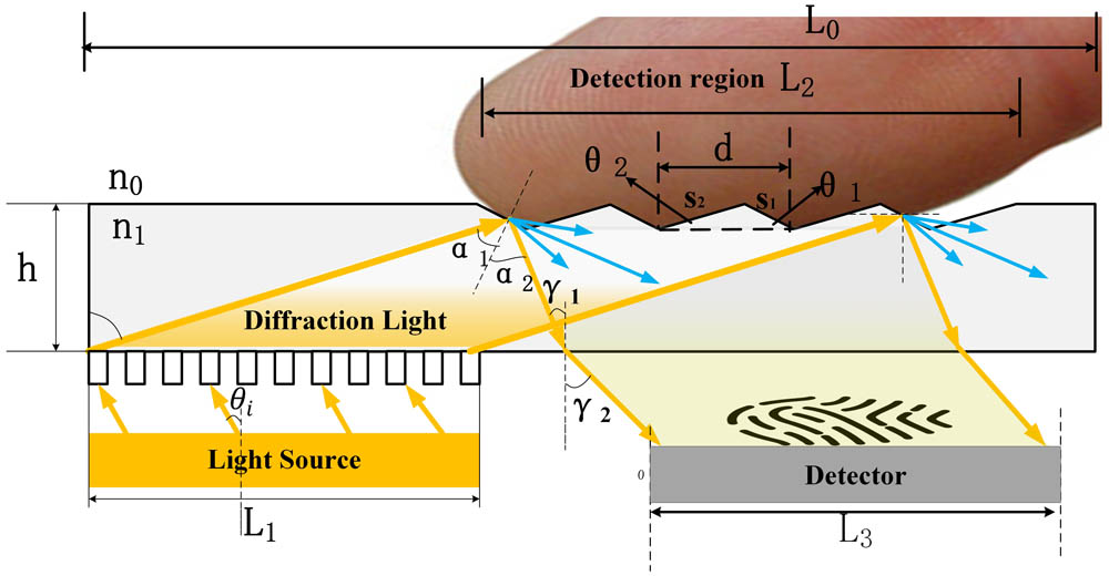
A schematic diagram of the proposed OFRS is depicted in Fig. 1, where the mechanism of our design structure is explicitly illustrated. A diffractive grating acts as an input element[14,15] to couple the collimated light into the planar waveguide with a certain propagation angle, according to the diffraction equation where is the pitch of the grating; and are the refractive indices of circumstance medium and optical waveguide, respectively; is the diffraction order; and are the incident angle and diffraction angle in the planar waveguide; is the wavelength of the incident light. Thus, the st order of diffraction angles satisfy the condition:
Sign up for Chinese Optics Letters TOC. Get the latest issue of Chinese Optics Letters delivered right to you!Sign up now
Figure 1.Geometry of the planar waveguide with the microprism array. , , , and are the length of the total OFRS, grating, microprism array, and width of detector; is the thickness of the planar waveguide; and are the refractive indices of the circumstance medium (air) and the optical waveguide, respectively; is the width of the single microprism; and and are the slope angles of the two facets and , respectively.
As shown in Eq. (2), the diffraction angle increases with the shortening of pitch . When is larger than the TIR angle between the waveguide and air, the diffraction light becomes waveguide modes totally reflected between the bottom and top boundaries of the planar waveguide. Thus the TIR condition of is satisfied, where is the refractive index of a normal finger. Generally, the thinner the planar waveguide, the more times the light beams are reflected by the waveguide boundaries for a specific diffraction angle. However, the light beams should irradiate the detection region only once, otherwise the fingerprint image carried by the reflected light will overlap and interfere with each other, and thus cannot be discriminated. Keeping a thin waveguide plate without image overlapping means that the diffraction angle should be large enough to make only one shot of the waveguide light on the detection region. Unfortunately, if the diffraction angle is larger than the TIR angle between the finger ridges and the optical waveguide, it would be very difficult to frustrate the TIR to get discernible finger images. In short, there is a contradiction between slimness and high contrast image output for the OFRS. The practical design given below can explain the mechanism more vividly, where the indices of the finger, air, and glass waveguide are [16], , and , respectively. Thus, we can get , and the thickness of the planar waveguide should be at least for a 15 cm width detection region, which is too thick. To decrease the thickness of the waveguide, we felicitously add an array of microprisms on the surface of the planar waveguide, as shown in Fig. 1, that can assist in destructing TIR by reducing the incident angle of diffracted light on the detecting surface. Notice that the detector in free space is close to the in-coupling grating on the same side but without images overlapping each other through an appropriate prism angle. The width constraints of the device are as follows:
When the light beams emitted from the light source reach the grating, they will be diffracted by a grating with a certain angle and directly strike the detection region. Then, some of the light beams will be reflected out of the planer waveguide and captured by the detector located beneath the waveguide. The simple geometric relationships of light propagation in the optical planar waveguide are described as follows:
In order to avoid fingerprint image aliasing, the microprisms should reflect the light beams directly to the detector without overstepping the boundary between the grating and the detector. It indicates that the width of the light source or the width of the grating will restrict the height of the waveguide to be larger. Notice that, in this condition, the thickness of the planar waveguide should be larger than the height of a single microprism. Thus, is limited by following formula:
According to Eq. (5), under a certain length of the grating, the larger the diffraction angle , the thinner the thickness of the planar waveguide, which means that a thinner device can be obtained. On the one hand, when a finger touches the detection region, as illustrated in Fig. 1, part of the light beams will be absorbed or scattered by finger skin. The forward scattering of finger skin shown as blue arrows is keeping away from the diffraction beams, thus a high contrast of the fingerprint pattern via reflection will be caught by the detector. On the other hand, when a finger is away from the detection region, the propagating light should be totally reflected by the microprism array, which means that the TIR condition between prism and air is satisfied: . To ensure that the light beams carrying fingerprint information can ultimately reach the detector, must be satisfied. From the above, the angle of the microprism should be restricted between the following ranges in combination with Eq. (4):
Note that is the prism angle corresponding to the angle between the waveguide plate and the side close to the light source. This side will not influence or interrupt the light rays, thus the following simple inequality should be maintained:
The efficiency of the above-mentioned structure was mainly determined by the diffraction efficiency of the grating and the characteristics of the microprism array. Thus, we simulated the parameters of the grating to optimize the diffraction efficiency using a finite difference time domain (FDTD Solutions, Lumerical). In order to rigorously illustrate the model and verify the feasibility of the proposed structure, we built a 3D geometric model of the fingerprint system using the commercial software LightTools, which traces the light beams based on the Monte Carlo method[17,18]. We will illustrate the procedures separately.
A conventional grating used as input coupler would separate the in-coupling light into order and then propagated along the waveguide in opposite direction. However, in most conditions, only one side of the diffraction light was serviceable while the other was extravagant. To further enhance the diffraction efficiency in one side of the grating, a slanted grating was used, as shown in Fig. 2. The slanted grating enlarges the efficiency of the st order diffraction, and decreases the 1st order diffraction efficiency at the same time. Thus, the st order diffraction light was fully utilized as detection light. Many parameters influenced the diffraction efficiency, among which the duty cycle (dc) and slant angle () of the grating, grating height, and morphology of the grating were the most important ones. In our simulation, the metal was aluminum, which was covered on the substrate to enhance the diffraction efficiency; the refractive index of the glass (NBK7, Schott) substrate and grating were 1.5 and 1.7, respectively; the period of the grating was 350 nm; and the light source was 5° oblique. Thus, the diffraction angle was 89° at , corresponding to the waveguide thickness of 260 μm (for ) or 174 μm (for ); the whole length of our structure was less than 30 mm; the minimum mesh step of the FDTD was 0.25 nm; 20 periods of the grating were taken in the simulation, and the perfect matched layer (PML) boundary condition was set in both the and directions; and the time step was , which is long enough for the incident light to pass the observation line completely. We used the control variable method to discuss the effect of the above-mentioned parameters on the change in diffraction efficiency. The initial parameters were: , , , , and . In each step of optimization, we change one parameter to the optimum value based on previous optimizing results.
Figure 2.Simulation model of a metallic grating. (a) 3D vision and (b) 2D vision of the front view. PR is photoresist (ARP 3500-6, Allresisit Co.). The symbols and represent the height of the grating and metal; represents the slant angle of the grating; and are the up and down length of the grating.
The simulated st order diffraction spectra varied with slant angle of grating lines, as shown in Figs. 3(a) and 3(b), which clearly indicate the optimized slant angle: . Under this slant angle, as illustrated in Figs. 3(c) and 3(d), the st order diffraction efficiencies are up to 70% for TE polarization and nearly 50% for TM polarization. The fill factor, grating height, and profile of grating lines will also influence the diffraction efficiency, but we will not discuss them in this Letter.
Figure 3.st order diffraction efficiency spectra of TE and TM polarized light with different parameters. Spectra of (a) TE and (b) TM polarized light with parameters: ; ; ; and . Spectra of (c) TE and (d) TM polarized light with in (a) and (b).
When a beam of light reached the surface of the finger skin, part of it would be reflected by the surface directly, while the rest would be transmitted into the skin and some of which would re-emerge into the air because of the scattering by the skin tissues. Thus, in the simulation, the finger was treated as a pillar distributed with microtexture on the surface, which represented fingerprints. The distance between two neighboring ridges and the height of the ridges were 0.5 and 0.05 mm, respectively. By measuring the intensity ratio between the incident light illuminated on one of the authors’ thumbs and the reflected beams, the reflection of the human fingers was regarded as a Lambertian body with a scattering of 35%, and the absorption was 65%, similar to previous work[19]. The refractive indices of the planar waveguide, fingerprint, and air are 1.5, 1.4, and 1.0, respectively. As mentioned before, our intention was to reduce the thickness of the waveguide under a certain length of detection region. Therefore, the diffraction angle should be as large as 90°, as illustrated in Eq. (5). To check the effect of this innovation, we set the first diffraction angle to 89°, which corresponded to the grating period for , and incident angle , thus the angle of the prism should be , as calculated by Eq. (6). In the following paragraphs, we will investigate the angles as well as , and the width of a single microprism; then we will obtain optimal parameters combining the fabrication and image quality; and in next section, we will discuss the tolerance of the manufacturing error.
For a prism, there are two facets and which are facing and along the diffracted lights. The facet plays a key role in changing the incident angle and its angle determines the effective sensing area. Thus, it is investigated first. The width of the singlemicro prism is one tenth of the width of the finger ridge, and . In the simulations, the luminance of the diffraction light was . The simulated results under different prism angles of are shown in Fig. 4. It is obvious that fingerprint patterns from the detector have high contrast image quality of , , , and corresponding respectively to , 25°, 30°, and 40°, which are much higher than for the previous report of [20].
Figure 4.Fingerprint images from the detector under prism angles and 40° while and .
With the increase of , more and more light beams escape from the prisms, which brings about the rising of noise in the fingerprint image and thus decreases the image contrast to when . In addition, we know that should be smaller for fingers to easily contact the prism facets fully; but on the other hand, the practical light source cannot emit an ideal collimated beam; a large angle of is required to prevent beam propagation in the planar waveguide. According to the above-mentioned reasons, is selected based on different divergence angles of light source, as follows:
The facet related to does not need to reflect the light beams directly, but would do better parallel to the direction of the diffracted light beams. As illustrated in Fig. 5(a), the blue zone is the effective contact region, which obviously declares that the larger degree of will block out transmitted light beams while a smaller degree will reflect transmitted light beams to somewhere else. Thus, we did the simulations for , 1°, and 35° under the condition of and , as shown in Fig. 5(b). We can see that 1° is the perfect angle for since it is not too large to influence the contact of the finger or too small to influence the luminance of the fingerprint images, which perfectly agrees with what we expect.
Width of a single prism plays the same role as to guarantee the details of the fingerprint image. The simulation results while and under different microprism widths of 0.05, 0.07, and 0.1 mm are shown in Fig. 6. The fingerprint images have some stripes as the width of the singlemicro prism becomes larger because of the rising difficulty for the finger range to touch the bottom of the microprism array. However, taking into account the cost and difficulty of fabricating small width prisms, as well as the image quality, a width of 0.05 mm is appropriate and feasible, meaning that the height of the single microprism is 3.68 μm, which is perceptually invisible for human beings.
Figure 5.(a) The light paths for different values of , (b) the fingerprint images from the detector under , 1°, and 35° while and .
Those parameters that we have discussed for , , and cannot strictly equal to we designed in real conditions. Thus, the mismachining tolerance should be considered. When the light source beams are divergent, some of the light beams can not couple into the waveguide, while others will reach the detector, thus the image becomes slightly distorted. But due to the angle sensitivity of the in-coupling grating, some light beams with a large incident angle will not couple in the waveguide mode, thus the contrast of the fingerprint images still remains over 65% even if the divergence angle becomes larger than 10°, as shown in Fig. 7. By considering both the image quality and light source cost, a divergence angle no more than 5° is allowed, which is not a matter of question as a divergence angle less than 0.5° is widely available[21]. In fabrication, the vertex angle of the micro prismmay not be as sharp as ideal, and not every two contiguous microprisms may be tightly adjacent, as shown in Figs. 8(a) and 8(b). All of these irresistible factors may cause the deformation or fuzziness of fingerprint images, as shown in Figs. 8(c) and 8(d). The fingerprint images become blurred and hard to recognize because of the round-shaped vertex angle of the microprism, while the pitch between the two microprisms bring stripes into the fingerprint image, which will reduce the image contrast. The results also show that the tolerance of the pitch distance is smaller than 0.03 mm while the corner radius is less than 0.01 mm to make sure the image contrast reaches 80%.
Figure 7.Fingerprint images from the detector under different divergent angles of light source, with , , and .
Figure 8.Profile of the microprism with: (a) ideal angle and non-gap; (b) non-sharp vertex angle and a small gap between two adjacent microprisms. Fingerprint images from two sensors while the microprisms are not ideal: (c) the corner radius is 0.01 mm and (d) the distance between two microprisms is 0.03 mm.
An OFRS with a high image contrast, fidelity, and thin planar waveguide is designed and discussed in this Letter. We demonstrate that the contradiction between the waveguide thickness and large diffraction angle is resoluble with the proper parameters of the grating and microprism array. Our idea of inserting a microprism array makes it possible to operate at a slim waveguide while aiming at a large diffraction angle. With the typical parameters, we can get the fingerprint image contrast up to 950:1 especially when , , , and the thickness of the waveguide is 260 μm for , which can be even thinner by increasing the diffraction angle or decreasing the length of detection region . In the meanwhile, the novel OFRS has a high tolerance with the collimation of light and fabrication error, which diminishes the cost and difficulty of manufacturing. In view of this, we can foresee a bright future for our OFRS in mobile terminal applications.
References
[1] S. Memon, M. Sepasian, W. Balachandran. IEEE International Multi-Topic Conference INMIC, 226(2008).
[4] J. K. Schneider, S. M. Gojevic. Proceedings of the IEEE Ultrasonics Symposium, 1, 595(2001).
[5] A. K. Tamhankar. Masters Abstracts International, 44, 1388(2006).
[6] Y. Ni. Optical imaging device for the recognition of finger prints. U.S. patent(2010).
[7] L. N. Darlow, S. S. Akhoury, J. Con-nan. Third International Conference on Digital Information, Networking, and Wireless Communications (DINWC), 188(2015).
Ping Ma, Xuecheng Cui, Jun Zheng, Pinchun Kang, 志成 叶. Slim OFRS based on a grating input coupler and a microprism sensing surface[J]. Chinese Optics Letters, 2016, 14(11): 112303