Alloying in two-dimension has been a hot spot in the development of new, versatile systems of optics and electronics. Alloys have been demonstrated to be a fascinating strategy to modulate the chemical and electronic properties of two-dimensional nanosheets. We firstly reported ultra-broadband enhanced nonlinear saturable absorption of Mo0.53W0.47Te2 alloy at 0.6, 1.0, and 2.0 μm. The nonlinear saturable absorption of Mo0.53W0.47Te2 saturable absorber (SA) was measured by the open aperture Z-scan technique. Compared to MoTe2 and WTe2 SAs, the Mo0.53W0.47Te2 SA showed five times deeper modulation depth, 8.6% lower saturable intensity, and one order larger figure of merit. Thus, our research provides a method of alloys to find novel materials with more outstanding properties for optics and optoelectronic applications.
Two-dimensional (2D) transition metal dichalcogenides (TMDs) have attracted considerable attention for nanoelectronic and optoelectronic applications because of their attractive carrier mobility, adjustable bandgap, light–matter interaction, and stable chemical properties[1–3]. The similar structure of (, , , , , etc.) is that the transition metal (M) atoms are sandwiched between two layers of chalcogen atoms (X). TMDs are the molecular layers formed by strong intra-layer chemical bonding and the weak van der Waals forces inter layer. The layered structure allows us to use top-down exfoliation to obtain mono- and few-layer nanoflakes by mechanical or chemical processes. The electronic properties of TMDs vary from semiconducting to metallic due to the precise elementary composition and geometry[4,5]. The semiconductors of TMDs can potentially serve as saturable absorbers (SAs), such as molybdenum disulfide and tungsten disulfide SAs, which already exhibit promising applications with much deeper modulation depth than graphene, but only in the visible range[6–8]. The semi-metallic property of TMDs such as extends the SA working band, but the modulation depth is relatively low due to its stronger reflection of excitation light[4,5]. To obtain novel SAs with more outstanding properties is the goal of SAs research.
TMD alloys provide a reasonable approach to tailor their physical and chemical properties. Element doping in TMD alloys is a substitutional doping rather than dopants occupying interstitial and defect sites[9,10]. The different phases and electronic structures of TMDs facilitate us to obtain adjustable, broadband, and optimized properties by alloying. Several ultra-thin ternary TMDs have been successfully prepared[11,12] (e.g., and ). However, only a few hundred milli-electron volts (meV) can be tuned, i.e., 80 meV for and 170 meV for solid solutions, respectively. The with 2H phase shows the semiconductor properties, while the semiconducting (Td) shows a semi-metallic property, displaying giant magnetoresistance. Yu et al. experimentally showed that is 2H and 1Td structures for and 0.4[13]. On a similar note, a series of single crystals by the chemical vapor transport (CVT) method were synthesized[14,15]. The phase transition was obtained by controlling the chemical ratio of gradually changing from the 2H, β to the Td phase. was identified as the mixture phases of β and Td, which was due to the residual phase in the process of phase transition[14,15]. The β and Td mixture phases of can introduce extraordinary physical properties needed for in-depth study. Compared to 2D binary TMDs, the alloys showed unique advantages making them fundamentally and technically important in applications of optics and optoelectronics. Surprisingly, excellent nonlinear optics (NLO) properties of mono- and few-layer alloys were studied by Wang et al., where alloys showed lower saturable intensity and deeper modulation depth[16].
Here, we firstly report the ultra-broadband and enhanced nonlinear SA of ternary . Based on the nonlinear optical theory model of Z scan, SA showed five times deeper modulation depth, 8.6% lower saturable intensity, and one order larger figure of merit (FOM) than those of and SAs. Thus, our research provides a method of alloys for finding novel materials with more outstanding properties for optics and optoelectronic applications.
Sign up for Chinese Optics Letters TOC. Get the latest issue of Chinese Optics Letters delivered right to you!Sign up now
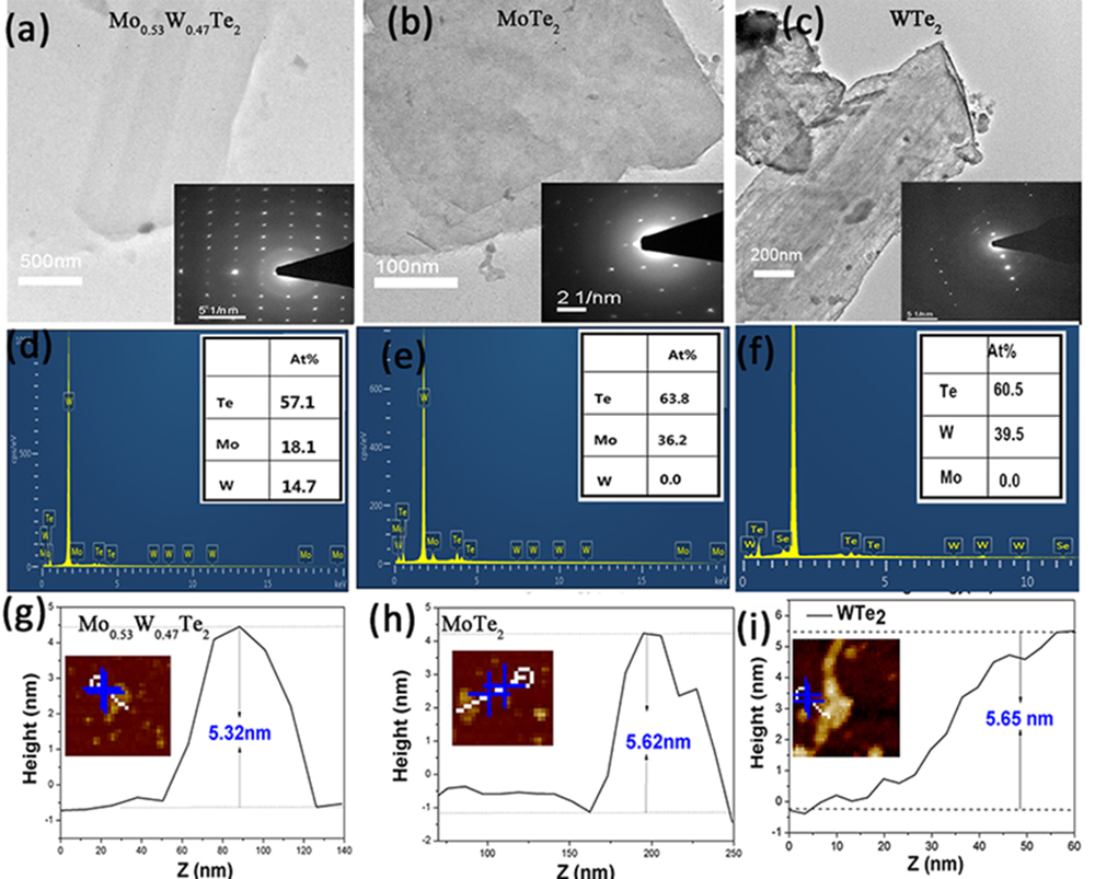
We prepared SAs by liquid-phase exfoliation and spin-coating technique in this work. For further comparison, the and SAs were treated by the same parameters in liquid-phase exfoliation and spin-coating processes[17]. Transmission electron microscopy (TEM) was employed to examine the morphology of the , , and . As shown in Figs. 1(a)–1(c), the layered structures of , , and could be seen, indicating that liquid-phase exfoliation was an effective method to obtain nanosheets. The spots of selected area electron diffraction (SAED) in the inset of Figs. 1(a)–1(c) indicated monocrystalline features of , , and nanoflakes. To identify the elemental ratio of the synthesized alloy, energy dispersive spectroscopy (EDS) was utilized. As shown in Figs. 1(d)–1(f), the chemical characterizations conformed to the stoichiometric ratio in the synthesis step. It can be seen that the ratio of Mo and W in was 0.53 to 0.47, indicating an efficient doping of W ions in the framework. Furthermore, atomic force microscopy (AFM) was employed to measure the three SAs’ thicknesses, as shown in Figs. 1(g)–1(i). The heights of , , and nanoflakes were about 5.32, 5.62, and 5.65 nm, corresponding to the number of layers of 8, 9, and 9, respectively.
Figure 1.TEM and SAED characterizations of few-layer nanosheets of (a) , (b) , (c) ; EDS spectra of (d) , (e) , (f) ; AFM images and data of (g) , (h) , (i) .
Raman spectroscopy was carried out to provide lattice vibration modes of synthesized . The study was carried out using a Jobin Yvon LabRam 1B Raman spectrometer with a laser at 532 nm. Figure 2 shows the Raman spectra of , , and β. The prominent peaks of the alloy can be defined as () and () modes based on the dominant direction of phonon vibrations. The mode of resulted from the corresponding modes in . The shift of mode was attributed to the significant changes in the electron–phonon coupling softened by the binary component . The frequency shift of at the mode of originated from the extra strain due to the different atomic radius of W and Mo. The showed multiple peaks of the β and Td-phase, indicating that was a mixture of phases β and Td, which may be formed due to the residual phases after the phase transition. The reflectance spectrum of metallic showed significantly enhanced light absorption over a wide range of wavelengths due to strong absorption of . Furthermore, also had a relatively flat absorption curve with stronger absorption due to the combination of linear absorption of and . The showed two absorption peaks located at the wavelengths of 403 nm and 762 nm, which coincided with spin-orbit splitting. Based on the Lorentz–Drude model, the fitted lines of transmittance were dashed lines shown in Fig. 2(b). The refractive indexes of the three SAs shown in Fig. 2(c) were calculated by the relationship of Kramers–Kronig[16,18].
Figure 2.(a) Raman spectra of , , and . (b) Comparison of recorded transmittance spectra and corresponding fitted lines of , , and . (c) The refractive index of , , and based on the relationship of Kramers–Kronig.
We adopted the most popular open aperture Z-scan measurements to obtain the nonlinear optical response. Mode-locked lasers operating at 0.639, 1.060, and 2.0 μm with 80 MHz repetition rate and 175 fs pulse width were used to study the NLO behavior of the SA. The NLO response of nanosheets could be clearly seen in Fig. 3. The increase of transmittance was easily observed with the increase of laser intensity, resulting from the nonlinear saturable absorption effect.
Figure 3.Open-aperture Z-scan results of , , and at (a) 639 nm, (b) 1060 nm, and (c) 2 μm.
Based on the theory of NLO, the total absorption consists of a linear absorption coefficient and a nonlinear absorption coefficient . The absorption coefficient is expressed as
Based on Beer–Lambert law, the propagation equation format is shown as
By fitting the Z-scan data with Eqs. (1) and (2), we can obtain the of the and nanosheets. The imaginary part of the third-order NLO susceptibility and the FOM for the third-order NLO are represented as[10–12]where is the speed of light, is the laser light wavelength, and is the refractive index calculated by the relationship of Kramers–Kronig. Based on Eq. (1), we calculated the FOM in Table 1. Compared to graphene, graphene oxide, and (NMP) dispersions of , the FOM of was , five orders of magnitude larger[19]. The results showed the nanosheets exhibited excellent nonlinearity. Due to the value of FOM varied with the difference of SA thicknesses and the preparation processes, we carried out the Z scan on the same condition, and the three SAs were prepared by the same parameters of liquid-phase exfoliation and spin-coating technique. The FOM value of the SA was larger than those of and SAs, which indicated the enhanced nonlinear performance.
Sample
λ(μm)
n
α0(104cm−1)
αNL(103cm/GW)
Imχ(3)(10−6esu)
FOM(10−10cm·esu)
Is(GW/cm2)
As
Mo0.53W0.47Te2
0.639
5.7
3.07
−42.10
−26.287
8.562
1.82
6.50%
1.06
5.9
3.04
−65.10
−72.313
23.787
1.12
5.40%
2.0
7.1
3.05
−52.10
−168.366
55.202
2.8
4.20%
MoTe2
0.639
2.7
1.06
−4.71
−0.682
0.226
8.7
5.89%
1.06
0.33
1.08
−4.01
−0.014
0.013
12.9
4.30%
2.0
0.11
0.92
−2.97
−0.002
0.003
4.24
1.17%
WTe2
0.639
11.7
0.82
−1.31
−3.40
4.13
3.04
1.30%
1.06
11.6
1.08
−1.50
−6.46
5.97
4.43
2.21%
2.0
11.6
0.92
−1.46
−12.50
13.58
13.9
1.87%
Table 1. Optics Parameters of Mo0.53W0.47Te2, 2H-MoTe2, and WTe2
In another NLO theory model, transmittance of the nanosheets is expressed in the form of[6–8,19]where is the modulation depth, is the non-saturable components, is the saturable intensity, and is the incident light intensity. We fitted the Z-scan data with Eq. (5), and the modulation depth and saturable intensity were obtained, respectively. The results are illustrated in Table 1. It should be noted that compared to and SAs, saturation intensity and modulation depth of the SA were lower and deeper at 0.639, 1.060, and 2.0 μm. can reach the saturable station at intensities of 1.82, 1.12, and at the wavelengths of 0.639, 1.060, and 2.0 μm, respectively. Compared to the SA, the SA exhibited 8.6% lower saturable intensity at 1 μm. Compared to the SA, the SA exhibited five times deeper modulation depth at 0.639 μm. It was consistent with the stronger linear absorption, as shown in Fig. 2(b).
In conclusion, we firstly, to the best of our knowledge, report the ultra-broadband and enhanced nonlinear saturable absorption of ternary with mixture phases of β and Td. The SAED, EDS, and Raman spectra showed that the alloy nanosheets had good quality. The nonlinear saturable absorptions of the filmy SA were also measured by the open aperture Z-scan technique. SA showed five times deeper modulation depth compared to SA at 639 nm; the SA showed 8.6% lower saturable intensity and three-orders larger FOM compared to the SA at 1060 nm and 2 μm, respectively. Thus, our research provides a method to find novel materials with more outstanding properties for optics and optoelectronic applications.