Laboratoire de Nanotechnologie et d’Instrumentation Optique, Institut Charles Delaunay, CNRS-UMR 6279, Universite de Technologie de Troyes, CS 42060, 10004, Troyes, France
The eigenmodes analysis of Bloch modes in a chain of metallic nanowires (MNWs) provides a significant physical understanding about the light propagation phenomena involved in such structures. However, most of these analyses have been done above the light line in the dispersion relation, where the Bloch modes can only be excited with radiative modes. By making use of the Fourier modal method, in this paper we rigorously calculate the eigenmode and mode excitation of a chain of MNWs via the fundamental transverse magnetic (TM) mode of a dielectric waveguide. Quadrupolar and dipolar transversal Bloch modes were obtained in an MNW chain embedded in a dielectric material. These modes can be coupled efficiently with the fundamental TM mode of the waveguide. Since the eigenmodes supported by the integrated plasmonic structure exhibit strong localized surface plasmon (LSP) resonances, they could serve as a nanodevice for sensing applications. Also, the analysis opens a direction for novel nanostructures, potentially helpful for the efficient excitation of LSPs and strong field enhancement.
1. INTRODUCTION
Localized surface plasmons (LSPs) are surface electromagnetic modes associated with the collective oscillations of the conducting electrons at the boundaries of metallic nanoparticles (MNPs) [1]. They have been extensively studied in recent years due to their potential applications in optical sensing nanodevices [2]. This is because the resonance wavelength of the LSP is highly dependent on the geometry of the particle and on the refractive index of the surrounding medium. Furthermore, LSP modes provide a highly confined electromagnetic field that can be used to probe a very small volume of matter [3].
Light propagation through periodic arrays of MNP or metallic nanowires (MNWs) has already been demonstrated in several previous works [4–10]. This propagation mechanism is explained by LSP near-field coupling between consecutive particles excited at their dipolar resonances. Due to this coupling effect, the MNP or MNW chains can behave as a metallic waveguide.
The coupling effect can be well understood with an eigenmode scrutiny of the plasmonic modes in the MNP chain. However, the large majority of the analysis has been done above the light line in the dispersion relations [9–12], where the modes of the chain can be excited only with radiative modes, that is, from the free space or from the substrate. The longitudinal (L), transverse out-of-plane (T2) [12], and higher multipolar chain modes [13] are among the eigenmodes that are reported above the light line region.
Sign up for Photonics Research TOC. Get the latest issue of Photonics Research delivered right to you!Sign up now
In order to study the MNP mode excitation below the light line limit, MNP chains integrated on top of a dielectric waveguide have been proposed [14–16], but the choice of the incident transverse electric (TE) mode of the waveguide limits the excitation of one kind of chain mode, namely the transverse dipolar (T1) chain mode [17,18].
Here we study the modes supported by a periodic array of MNWs below the light line in the dispersion relation and their excitation with the fundamental transverse magnetic (TM) mode of a dielectric waveguide placed in close proximity of the MNW array. To do so, we first analyze the isolated MNW chain embedded in a homogeneous dielectric medium, then on top of a dielectric substrate, and finally approaching a dielectric waveguide. The analysis was done by using the Fourier modal method (FMM) for nonperiodic structures.
The paper is organized as follows: after a general presentation of the theoretical model, eigenmode dispersion relations are computed and analyzed for a MNW chain embedded in three different background media: (1) in a homogeneous glass medium, (2) on top of a silicon nitride substrate, and (3) on top of a silicon nitride waveguide. Finally, we deeply study a practical implementation of the latter structure with calculations on beam propagation and spectral responses.
The numerical results show that there is a mode coupling effect between the dielectric and the plasmonic waveguide, an effect that could be applied in the design of an integrated plasmonic sensing device.
2. NUMERICAL METHOD
The numerical method developed in this work is grounded on the so-called FMM, also known as rigorous coupled wave analysis (RCWA), which relies on a rigorous electromagnetic model based on the description of the Maxwell equations in the frequency domain. It is based on the Fourier series expansions of the dielectric function and the electromagnetic field [19]. With this formulation is possible to find the eigenmodes supported by a chain of MNPs of any shape immersed in a multilayered medium (its dispersion relations) and also to simulate the beam propagation through the structure. By making use of the effective index method, it is also possible to extend the numerical model into a three-dimensional simulation.
The general solution of this method involves two main steps:
Calculation of the eigenvalues and the eigenvectors of a matrix with constant elements that characterizes the diffracted wave propagation and coupling (the eigenvectors represent the characteristic modes of the periodic array) in a profile of the propagation axis, as well as the effective indices corresponding to these modes;
The resolution of a linear system deduced by the boundary conditions for normal and tangential components of the electric and magnetic fields to reconstruct the total field.
The characteristic matrix of the multilayered structure is the product of the characteristic submatrices in each layer. A detailed description of this method can be found in the work published by Chateau and Hugonin [19] and also in other references [20–23]. Here we mention only the generalities of the method. It must be remarked that we use the Fourier factorization rules proposed by Li [24], but in order to improve the numerical convergence, other methods can also be applied [25,26].
A. Dispersion Relations
Since the multilayered structure to be analyzed includes a periodic array of metallic nanowires, it supports Bloch electromagnetic eigenmodes. These modes can be calculated by solving the general solution of the Maxwell equations in the frequency domain as a sum of propagative and counterpropagative plane waves. Taking into account the invariance of the structure along the axis [Fig. 1(a)], the resulting Helmholtz equation for TE or TM polarization modes can be regarded as an eigenvalue problem. Using the boundary conditions for normal and tangential components of the field, the eigenmodes can be calculated with the scattering matrix algorithm [24] that associates the incoming and outgoing fields after the interaction with a multilayered structure with the relationship where is a matrix associated with the characteristic matrix and with the effective index, including the angle of incidence and the period of the structure, and are the incoming and outgoing fields in the th layer. The Bloch modes are then determined by finding the complex solutions of the relationship , where is the normalized propagation constant [5].
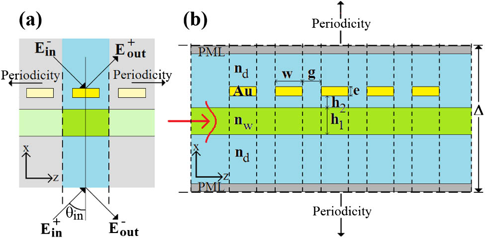
Figure 1.(a) Schematic representation of a unitary cell used for the calculation of the dispersion relations as an eigenvalue problem. The periodicity is along the axis. (b) Scheme for the calculation of the beam propagation. A unitary cell contains a finite number of nanowires along the propagation direction ( axis), and the periodicity is now along the axis including PMLs.
It must be noted that as we are working in the frequency domain for a single section of the structure, the Bloch modes are the solution of an infinite number of nanowires in the reciprocal space, bounded in the transversal direction.
B. Beam and Mode Propagation
For the propagation of the field under a particular guided mode excitation, we make use of a similar procedure than that used before, but in this case we compute the modes perpendicularly to the propagation axis. In other words, the periodicity of the structure and the Fourier transform are taken along the axis [Fig. 1(b)], and the number of nanowires is now finite.
The structure is subdivided into several sections invariant along the propagation direction. Then we include perfectly matched layers (PMLs) at the top and bottom of these sections in order to absorb the light scattered by the section and to avoid any reflections at the edges of the finite computational window of size . For each section, we compute the modes as an eigenvalue problem [19] with the use of a Fourier expansion of the permittivity and the electromagnetic field, and of R and S matrix algorithms [22]. The mode propagation through the structure is then a linear combination or Fourier expansion of different propagative as well as contrapropagative modes. Finally, the amplitudes of each mode at every section are calculated from the initial conditions at the edges of the structure and from the continuity of the tangential components of the electric and magnetic fields at the interface of two successive sections [24]. The method allows us to obtain the transmission and the reflection of the field along the dielectric waveguide as well as intensity maps of the electromagnetic field in the structure. The absorption is determined with the relationship [27]where is the imaginary part of the dielectric function. The components of the electric field can be determined from the magnetic field via
To normalize the absorption in Eq. (2), we divide it by the incident power given by for TE polarization, and for TM polarization. Although the method is valid for TE or TM polarized fields, we consider only the TM polarization to excite LSP resonances supported by the MNW.
3. NUMERICAL EXAMPLES
In order to validate the numerical method and to show its implementation in a stratified system, we present the results of the modal analysis for three cases. The first [Fig. 2(a)] consists of an infinite periodic array of gold nanowires of width , height , and period , immersed in a homogeneous glass medium with refractive index . The second case [Fig. 2(b)] corresponds to the same MNW array deposited on a dielectric substrate of refractive index closed to silicon nitride . Finally, the third example presents the dispersion analysis for the case of an integrated structure consisting of a silicon nitride waveguide of thickness and core refractive index , approached to a distance below the MNW chain [Fig. 2(c)]. The thickness and refractive index of the dielectric waveguide were previously calculated to support only the TM0 fundamental mode in a spectral range from 400 to 1500 nm. The values of the dielectric function of gold were taken from the list of Palik [28].
Figure 2.Schemes of (a) the periodical array of gold nanowires immersed in a homogeneous dielectric medium with refractive index . The height of the nanowires is , the width is , and the period is . (b) The same MNW chain on a substrate of refractive index , and (c) an integrated structure of MNW on a dielectric waveguide with core index .
The calculated dispersion relation of the MNW array immersed in a homogeneous medium with refractive index presents two Bloch modes [Fig. 3(a)]. As described in the previous section, the modes are solutions of the eigenvalue problem.
Figure 3.(a) Dispersion relations for the quadrupolar (upper branch) and dipolar transversal (lower branch) Bloch modes. The propagation distance of the (b) quadrupolar branch is shorter than that of the (c) dipolar transversal mode.
To identify the nature of each eigenmode branch, we calculated the energy density maps and their corresponding electric field lines distribution at the edge of the first Brillouin zone (at the Bragg condition) (Fig. 4). For the branch in the wavelengths range , we recognize periodic quadrupolar-like LSP excitations [Fig. 4(a)] with a phase shift of between adjacent nanowires, while for the second branch [], a dipolar-like LSP resonance perpendicular to the axis is observed [Fig. 4(b)]. This means that if the MNWs are excited at their LSP resonance, they behave as a waveguide system.
Figure 4.Energy density maps and electric field distribution at the Bragg condition for (a) the quadrupolar Bloch mode at and (b) the dipolar transversal Bloch mode at . The corresponding squares show the phase distributions and orientation of the charges.
The propagation distance () of the Bloch modes is obtained with the use of the equation , where is the imaginary part of the wave vector. As can be seen in Fig. 3(b), the propagation distance of the upper Bloch mode branch (quadrupolar mode) varies from 0.19 to 5.6 μm, while for the lower branch (transversal mode) the propagation distance is larger, varying from 4 to 31 μm.
We must remark that when the height of the nanowires is decreased, for example at (calculation not shown), the transversal Bloch mode [Fig. 4(b)] vanishes, and the quadrupolar Bloch mode [Fig. 4(a)] becomes a dipolar resonance parallel to the axis.
B. MNW Chain on a Substrate
When the MNW array is placed on a dielectric substrate () and surrounded with the same homogeneous dielectric medium (), we obtained three branches in the dispersion relations [Fig. 5(a)]. The ones at the top and the bottom are again related to the quadrupolar [Fig. 5(b)] and dipolar transversal [Fig. 5(d)] Bloch modes, respectively. They are, however, shifted in spatial frequency relative to those of the isolated MNW array because of the presence of the substrate, which induces changes in the wave vector.
Figure 5.(a) Dispersion relation of the MNW chain on a dielectric substrate (, ). The top and bottom branches belong to the quadrupolar and transversal Bloch modes, respectively. The middle branch corresponds to the excitation of the SPP at the interface between the metallic nanowires and the substrate. Energy density maps and electric field distributions at the Bragg condition for (b) the quadrupolar mode at , (c) the SPP-like mode at , and (d) the dipolar transversal mode at . The charge distribution in (c) exhibits a dipolar longitudinal interaction between the MNW only at the metal–substrate interface.
The middle branch belongs to the excitation of a surface plasmon polariton (SPP)-like mode. This is because the applied field induces longitudinal dipoles at the metal–substrate interface, and since the separation of the MNWs is smaller than their width (), a dipolar interaction arises between them, like in a metallic layer [Fig. 5(c)]. This resonance only exists when the light propagating in the MNPs and in the dielectric medium have the same wave-vector values. In this case, this condition is only achievable when the resonance is below the light line of the substrate, and this is why the branch exhibits a cutoff just at this limit.
The previous results suggest that if a dielectric waveguide is approached to the structure, it is possible to have a directional coupling between the modes of the MNW chain and the modes of the dielectric waveguide, as will be discussed in the next numerical example.
C. MNW Chain in an Integrated Structure
From the previous results, we concluded that under certain conditions, the MNW chain behaves as an optical waveguide supporting Bloch modes. These modes can be coupled to the modes of a dielectric waveguide placed in close proximity to the MNW chain if their respective vectors match at a fixed wavelength.
In the dispersion curves of Fig. 6, the upper branch of the Bloch modes crosses the fundamental TM0 mode of the dielectric waveguide at (), so their vectors are matched. Therefore, like in a coupled waveguide system, antisymmetric and symmetric supermodes are generated around this wavelength value. This anticrossing phenomenon is typical of a directional coupler, so we expect to have a periodical energy beating between the modes supported by the MNW chain and the mode supported by the waveguide. Although the vectors of the dipolar transversal branch and that of the TM0 mode of the dielectric waveguide do not match, an energy exchange between the MNW chain and the dielectric waveguide could be expected. The reason is that the leaky modes of the dielectric waveguide could interfere with the transversal mode of the chain of gold nanowires as its field is a highly confined field between the nanowires. This phenomenon is demonstrated in the next section.
Figure 6.Dispersion curves of the integrated structure (red lines), the isolated dielectric waveguide (blue), and the isolated MNW chain (green lines). The quadrupolar Bloch mode (inset) is coupled to the dielectric waveguide at , generating antisymmetric and symmetric supermodes. The dipolar transversal mode does not cross the fundamental TM0 mode of the dielectric waveguide.
As was previously demonstrated, the MNW chain supports quadrupolar and dipolar transversal Bloch modes. The dispersion curves reveal that an efficient directional coupling with a dielectric waveguide is expected with the quadrupolar branch. For the dipolar transversal mode, the field is confined between the nanowires, so an energy beating with the evanescent field of the dielectric waveguide is also expected.
Since the numerical method allows us to determine the beam propagation through the integrated structure, a deeper study of the integrated structure can be realized. To this purpose, we calculate the normalized transmission and reflection at the input and output of the dielectric waveguide, as well as the absorption of the structure in a spectral range from 400 to 1500 nm. Near-field maps of the amplitude of the component of the TM polarized light were calculated to prove the energy exchange. As the beam propagation method based in the FMM is periodic along the axis, the number of nanowires now is finite. For this case we use a finite chain of 27 MNWs.
The spectral curve of Fig. 7 shows the normalized transmission, reflection, and absorption of the complete system. The reflection curve (blue dashed) exhibits three main maxima at , , and . They correspond respectively to the Bragg reflection conditions of the quadrupolar (antisymmetric and symmetric) and transversal dipolar branches (red lines in Fig. 6). This can be verified with the expression , where is the effective index of the guided mode, the period of the chain of nanowires, and the Bragg order. For example, from the dispersion curve, the Bragg reflection of order for the dipolar transversal mode has an effective index , giving , which is the value of the third maxima in the main reflection band. These reflections induce two minima in the transmission curve at and at .
Figure 7.Transmission, reflection, and absorption spectra for the integrated structure. In the transmission curve, the quadrupolar mode is excited at , and the constructive interference of the dipolar transversal mode is positioned at . The minimum at is a cavity resonance effect. In the reflection curve, Bragg reflections are located at , , and at .
Efficient excitations of the quadrupolar and dipolar transversal MNW chain modes are observed respectively at and at in both transmission and absorption spectra. For the first one, a directional coupling takes place, since an anticrossing phenomenon appears in the dispersion curves between the waveguide fundamental TM0 mode and the quadrupolar MNW branch. In Fig. 8(a) this coupling effect can be confirmed, since a vertical periodic energy beating from the dielectric waveguide to the MNW chain is clearly observed. From the coupled mode theory, the spatial half-period of the coupling length can be estimated by , where is the effective index difference between the symmetric and antisymmetric modes at a given wavelength , and from the dispersion curves, the calculated effective indices are and , resulting in a coupling length of .
Figure 8.Amplitude maps of the component of the electromagnetic field corresponding to (a) the excitation of the quadrupolar mode () and (b) the interference of the dipolar transversal mode with the fundamental TM0 mode of the dielectric waveguide at .
Concerning the excitation of the dipolar transversal mode, the directional coupling is not the main process since no anticrossing phenomena occur in the dispersion curves. Nevertheless, as is depicted in Fig. 8(b), close to , the TM0 launched mode is coupled to the array of nanowires. A vertical energy beating is still visible (weakly contrasted) in the intensity map and is attributed to an interference patterns between guided and leaky modes. Indeed, the beating period at a given wavelength in a two-waveguide coupling system can be obtained via , where are the effective indices of the modes supported by the coupled waveguides. From the dispersion curves, at , , and from the intensity map the beating period is 1.17 μm, which results in a leaky mode effective index (above the light line in the surrounding medium ). The transmission spectrum changes abruptly (between and ) as a result of the interference between multiple reflections at the edges of the array. The wavelength separation between adjacent transmission minima is given by , where is the central wavelength, μ is the cavity length, and is the effective index. The calculated agrees with the value obtained from the transmission spectrum for the two minima located at 990 and 1055 nm ().
Also, as was previously predicted in the plots of Fig. 3, the propagation distance of the quadrupolar Bloch mode is shorter than the one of the dipolar transversal mode.
5. CONCLUSIONS
With the use of the FMM for stratified mediums, we calculated the dispersion relation of the Bloch modes in a chain of MNWs integrated on top of a dielectric waveguide. A quadrupolar and a dipolar transversal LSP Bloch mode were found along the MNW chain. When the nanowires are placed on a substrate, a third resonance branch arises below the substrate light line due to the excitation of an SPP at this interface which is also a propagation mode. Besides the dispersion relation, the numerical method allowed us to obtain near-field maps as well as to compute the transmission, reflection, and absorption spectra.
We demonstrated that the MNW chain behaves as a waveguide for LSPs, whose modes can be excited with the fundamental mode of a dielectric waveguide. A coupling of the energy inside the nanowire array is achievable with short coupling lengths even without perfect matching of the wave vectors.
Since the eigenmodes supported by the nanowires exhibit strong LSP resonances, the analyzed structure may serve as a nanoscale integrated device for sensing applications, useful for biological or chemical detection in Raman or localized surface plasmon resonance spectroscopy methods.
The proposed integrated structure opens a direction for new optical waveguide designs, potentially helpful on the efficient excitation of LSPs and strong field enhancement.
References
[1] C. Bohren, D. Huffman. Absorption and Scattering of Light by Small Particles(1998).