• Journal of Semiconductors
  • Vol. 41, Issue 12, 122301 (2020)
Zhihua Yin, Xuemeng Hu, Jianping Zeng, Yun Zeng, and Wei Peng
Author Affiliations
  • Key Laboratory for Micro/Nano Optoelectronic Devices of Ministry of Education & Hunan Provincial Key Laboratory of Low-Dimensional Structural Physics and Devices, School of Physics and Electronics, Hunan University, Changsha 410082, China
  • show less
    DOI: 10.1088/1674-4926/41/12/122301 Cite this Article
    Zhihua Yin, Xuemeng Hu, Jianping Zeng, Yun Zeng, Wei Peng. Self-powered circularly polarized light detector based on asymmetric chiral metamaterials[J]. Journal of Semiconductors, 2020, 41(12): 122301 Copy Citation Text show less

    Abstract

    Circularly polarized light (CPL) has been given great attention because of its extensive application. While several devices for CPL detection have been studied, their performance is affected by the magnitude of photocurrent. In this paper, a self-powered photodetector based on hot electrons in chiral metamaterials is proposed and optimized. CPL can be distinguished by the direction of photocurrent without external bias owing to the interdigital electrodes with asymmetric chiral metamaterials. Distinguished by the direction of photocurrent, the device can easily detect the rotation direction of the CPL electric field, even if it only has a very weak responsivity. The responsivity of the proposed detector is near 1.9 mA/W at the wavelength of 1322 nm, which is enough to distinguish CPL. The detector we proposed has the potential for application in optical communication.

    1. Introduction

    Recent investigations on optical communication[1], optical image processing[2], and biomedical diagnosis[3] have indicated the significance of circularly polarized light (CPL). In CPL, the electric field vector, which can be decomposed into two linearly polarized components with perpendicular electric field vectors that are oscillating with a 90° phase shift, travels along a helical trajectory with a clockwise or counterclockwise direction[4]. CPL can be classified as left-handed circularly polarized (LCP) light and right-handed circularly polarized (RCP) light, due to the differently helical trajectory of the electric field vectors. Although distinguishing CPL can be realized by the combination of several optical elements in conventional optics, it is too complicated and inconvenient in practical application. Campbell et al. demonstrated a chiral organic semiconductor transistor for CPL detection with a highly specific photoresponse at 365 nm in 2013, which can be miniaturized and integrated as ultra-compact devices[5]. In 2019, Tang et al. also reported a CPL photodetector employing chiral hybrid perovskite with a responsivity of 797 mA/W at a wavelength of 395 nm[6]. Further, they exhibited that the photodetector for CPL detection has one-month stability.

    The chirality of chiral metamaterials is currently the most popular method for CPL detection. Researchers are very interested in special properties of chiral metamaterials, such as circular dichroism (CD), optical rotatory dispersion (ORD), Raman optical activity (ROA)[7]. Many devices with chiral metamaterials have been presented in the literature, such as gammadion-shaped nanostructures[8], spiral-shaped molecules[7], double-layered metallic U-shaped cells[9], and bilayered chiral metamaterials[10]. Moreover, chiral nanowires with a strong circular dichroism spectrum also have been studied[11, 12].

    In general, self-powered devices have more potential because of their economy and adaptability than those with external power in practical applications. Most self-powered devices based on heterojunctions[13], Schottky junctions[14], or organic/inorganic hybrid pn junctions[15], which separates the electron–hole pairs rapidly by a built-in electric field[16] that have been developed rapidly in recent years. In particular, self-powered photodetectors of Schottky junction formed by chiral metamaterials and semiconductors have indicated a great potential to detect CPL. The CPL detector with chiral plasmonic metamaterials was reported by Valentine et al.[4], who realized an ultracompact optical element successfully and obtained perfect optical absorption toward CPL at a communication wavelength of 1340 nm excellently.

    In this paper, we propose and optimize self-powered photodetectors based on chiral interdigital structure, which is a new type of device that can detect CPL through the direction of photocurrent at zero bias. The performance of CPL detection will be good for the devices, even if we do not chase high responsivity. The rotation direction of the CPL electric field can be distinguished by the direction of photocurrent in these devices. The self-powered photodetectors that we propose in this paper are more economical and adaptable than the conventional ones.

    2. Structure and physical model

    Generally, the higher the responsivity is, the better the performance of conventional devices that detect CPL by the magnitude of photocurrent will be[4-6, 11, 12]. However, it is not easy for conventional photodetectors to improve responsivity. In this paper, we propose a new kind of CPL detector. Distinguished by the direction of photocurrent, the device can easily detect the rotation direction of the CPL electric field, even if it only has a very weak responsivity.

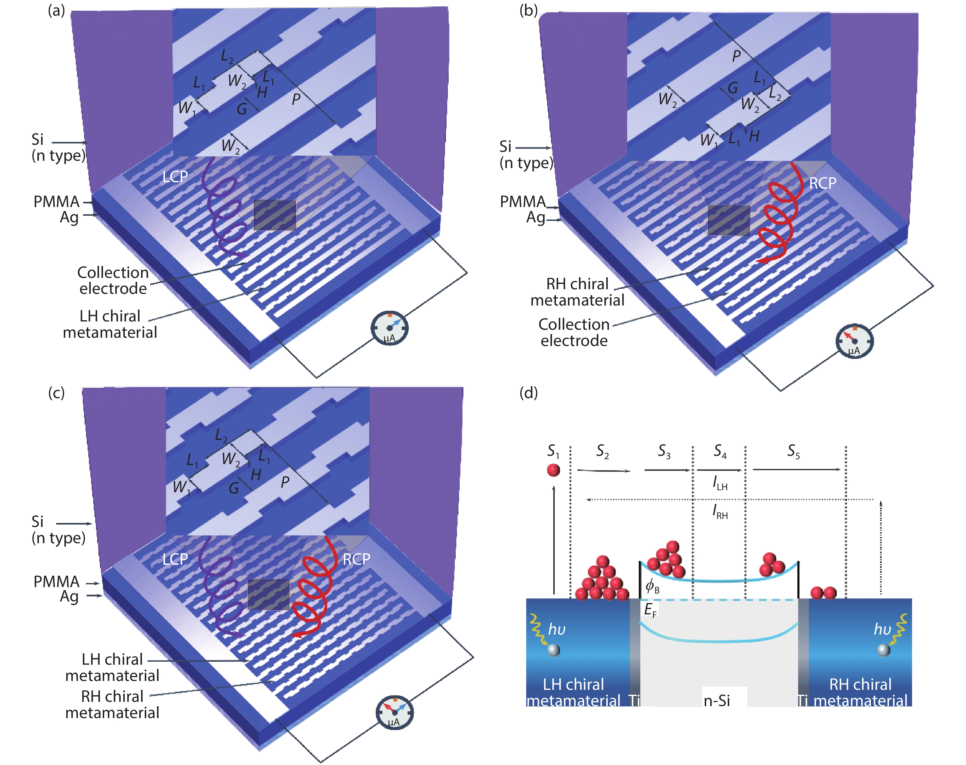
    Herein, we propose three kinds of devices based on interdigital structures with chiral metamaterial electrodes, as shown schematically in Figs. 1(a)1(c). These devices are designed by placing an n-type silicon wafer (500-µm thick) in contact with the Ag antenna layer, which is on top of a poly (PMMA) spacer. It should be noted that there is a 1-nm-thick layer of Ti between the silicon and Ag antenna layer, which can lower the Schottky barrier and enhance the adhesion of nanoelectrodes. The bottom layer is an Ag backplane used as a reflector for reflecting the incident light back to the nanoelectrodes and then can enhance the optical absorption and CD of ‘Z’ shaped metamaterial[4].

    (Color online) The thickness of antenna layer, dielectric spacer (PMMA) and Ag backplane are 40, 160, and 100 nm, respectively. The dimensions of the chiral-molecules are L1, L2, W1, W2, P, H, G, and 105, 230, 85, 115, 470, 40, 120 nm, respectively. (a) Schematic illustration of a device with an interdigital structure composed of left-handed (LH) chiral metamaterials and stripe antenna in device 1. (b) An interdigital structure composed of stripe antennas and right-handed (RH) chiral metamaterials in device 2. (c) An interdigital structure composed of left-handed (LH) chiral metamaterials and right-handed (RH) chiral metamaterials in device 3. (d) Band diagram of the device, of which photocurrent generated in five consecutive steps. A Schottky barrier formed by Si and Ti.

    Figure 1.(Color online) The thickness of antenna layer, dielectric spacer (PMMA) and Ag backplane are 40, 160, and 100 nm, respectively. The dimensions of the chiral-molecules are L1, L2, W1, W2, P, H, G, and 105, 230, 85, 115, 470, 40, 120 nm, respectively. (a) Schematic illustration of a device with an interdigital structure composed of left-handed (LH) chiral metamaterials and stripe antenna in device 1. (b) An interdigital structure composed of stripe antennas and right-handed (RH) chiral metamaterials in device 2. (c) An interdigital structure composed of left-handed (LH) chiral metamaterials and right-handed (RH) chiral metamaterials in device 3. (d) Band diagram of the device, of which photocurrent generated in five consecutive steps. A Schottky barrier formed by Si and Ti.

    In Fig. 1(a), the ‘Z’-shaped unit cells of the left-handed (LH) chiral antennas allows for an integral electrical connection among all the elements, forming a chiral nanowire[4]. The collecting electrodes are silver stripe antennas[17]. LH chiral nanowires and stripe nanowires are interdigital arrangements in antenna layer. LH chiral metamaterials, where the chirality suppresses the refractive index of RCP light and enhances the refractive index of LCP light through multiple reflections[4, 18], are selective to LCP light. LH chiral metamaterials serve as light collectors and electron emitters in device 1, while stripe antennas function as electron collection electrodes. Light absorption in plasmonic LH chiral metamaterials can be further enhanced by exciting localized surface plasmon resonances (LSPRs). A large amount of hot electrons generated from the non-radiative decay of surface plasmons on LH chiral metamaterials under LCP light illumination can be harvested with metal–semiconductor Schottky interfaces, and collected by stripe antennas finally, leading to current[19]. The current from LH chiral metamaterials to collecting electrodes can be detected by post circuits, which can be regarded as the signal of distinguishing LCP light by the direction of photocurrent. But LSPRs will be hardly excited due to LH chiral metamaterials that are insensitive to incident RCP light. We can assume that the pointer (blue) of sensitive galvanometer deflects for LCP light as shown in Fig. 1(a), but the pointer of sensitive galvanometer barely deflects for RCP light. Similarly, device 2 with an interdigital structure composed of right-handed (RH) chiral antennas and stripe antennas can be graphically visible to Fig. 1(b). The current flows from RH chiral metamaterials to collecting electrodes in post circuits, which can be deemed as the signal of distinguishing RCP light. This characteristic can be explicitly depicted by Fig. 1(b) where the pointer (red) of sensitive galvanometer deflects under RCP light illumination.

    Although these two devices (device 1, device 2) have unique advantages for CPL detection by the direction of photocurrent, it is only clearly sensitive to LCP or RCP for a single device. The optimized device, which integrates functional advantages of the above two devices while overcoming their respective drawbacks, can be seen in Fig. 1(c). The interdigital structure is composed of LH chiral metamaterials and RH chiral metamaterials. On the one hand, LSPRs can be induced by LCP light on the LH chiral metamaterials, which generates a large amount of hot carriers forming concentration gradient, and the diffusing hot electrons are collected by RH chiral metamaterials. In post-circuit, the current from LH chiral metamaterials to RH chiral metamaterials can be detected. On the other hand, hot carriers created from the RCP light absorption of RH chiral metamaterials are injected into semiconductor and then collected by LH chiral metamaterials, resulting in current from RH chiral metamaterials to LH chiral metamaterials in post-circuit.

    To understand clearly how the device distinguishes CPL by the direction of photocurrent, we can depict that the pointer (blue) of the sensitive galvanometer turns right under LCP light illumination as shown in Fig. 1(c). In contrast, the pointer (red) turns left under RCP light illumination. Thus, LCP and RCP light can be distinguished by the opposite direction of photocurrent clearly.

    For the optimized device, the generation of photocurrent amid hot electrons across a barrier can be described by five physical steps shown in Fig. 1(d)[20, 21]. In the first step (S1), when CPL light incident from the front and reflected from the backplane is superimposed on the antenna layer, the LH chiral metamaterials absorb photons of a particular handedness[4]. Hot electrons can be generated in LH chiral metamaterials by the absorption of photons with energy . This process of exciting hot electrons will be depicted by the finite-difference time domain method (Lumerical FDTD Solutions) later.

    In the second step (S2), hot electrons reach the Ag–Si interface with kinetic energy as shown in Fig. 2(a). The kinetic energy is given by Eq. (1)[21]:

    (Color online) (a) Cross-section of the k-space distribution of the Ag-Si interface. (b) Emission probability of a hot carrier with reflecting events.

    Figure 2.(Color online) (a) Cross-section of the k-space distribution of the Ag-Si interface. (b) Emission probability of a hot carrier with reflecting events.

    ${E_{{\rm{K}},{\rm{Ag}}}} = {E_{{\rm{F}},{\rm{Ag}}}} + E = \frac{{{\hbar ^2}}}{{2m_{\rm{e}}^*}}k_{{\rm{Ag}}}^2.$ (1)

    Here, is a Fermi level of Ag, is the reduced Planck’s constant, is the effective mass of the electron. The total momentum of a hot electron is given by Eq. (2):

    $k_{{\rm{Ag}}}^2 = k_{{\rm{Ag}},x}^2 + k_{{\rm{Ag}},{{y}}}^2,$ (2)

    where and are the hot electron momenta of LH chiral metamaterials in the x and y directions respectively. Once the electron is injected into the Si substrate, its kinetic energy and momentum will change relatively. The kinetic energy can be given by Eq. (3):

    ${E_{{\rm{K}},{\rm{Si}}}} = E - {\Phi _{\rm{B}}} = \frac{{{\hbar ^2}}}{{2m_{\rm{e}}^*}}k_{{\rm{Si}}}^2,$ (3)

    where is the height of the Schottky barrier, which is formed on the interfacial layer between Si and Ti[19], is the total momentum of a hot electron in Si substrate and calculated as Eq. (4):

    $k_{{\rm{Si}}}^2 = k_{{\rm{Si}},x}^2 + k_{{\rm{Si}},y}^2.$ (4)

    In the third step (S3), some hot electrons transfer across the Schottky barrier and traverse the Ag–Si interface with a certain probability. Hot electrons can escape only when , which limits emission probability to a solid angle . Thus, emission probability is given by Eq. (5):

    $P(E) = \frac{{\int_0^{2\pi } {\int_0^\Omega {\sin } } \theta {\rm d}\theta {\rm d}\phi }}{{4\pi }} = \frac{1}{2}(1 - \cos \Omega ).$ (5)

    Some hot electrons reaching the Ag–Si interface may be reflected, while the others may traverse the Ag–Si interface after multiple scattering events in Fig. 2(b). Therefore, we make two assumptions[20, 22, 23], as follows: (1) if hot electrons cannot traverse the Ag–Si interface, they will get to the interface in an elastic collision; and (2) electrons cannot travel through the vacuum interface or escape into the vacuum, but they can get to the interface in an elastic collision. The probability when reflecting N times can be calculated as Eq. (6)[23]:

    $\left\{ {\begin{array}{*{20}{c}} \!\!\!\!\!\!\!\!\!\!\!\!\!\!\!\!\!\! {P(E) = \dfrac{1}{2}(1 - \cos \Omega ),\quad \;\;{\rm{ when }}\;N = 0}, \\ \!\!\!\!\!\!\!\!\!\! {P(E) = {P_0} + \left( {1 - {P_0}} \right){P_1} + \left( {1 - {P_0}} \right)\left( {1 - {P_1}} \right){P_2}} \\ \quad\qquad\!\! { + \cdots + {P_N}\prod\limits_{m = 0}^{N - 1} {\left( {1 - {P_m}} \right)} ,\;\;\;{\rm{ when }}\;N \gt; 0}, \end{array}} \right.$ (6)

    where is the emission probability of a hot electron within LH chiral metamaterials after traveling an N-number of round trips[24].

    ${P_N} = \frac{1}{2}\left( {1 - \sqrt {\frac{{{\Phi _{\rm B}}}}{{{E_0}{\rm{e}^{ - \frac{{2NH}}{L}}}}}} } \right),$ (7)

    where L is the mean free path of the electrons[25]. H is the height of LH chiral metamaterials. is the initial energy of the hot electrons, and is the Schottky barrier. The total number of round trip N is given by Eq. (8):

    $N = \frac{L}{{2H}}{\rm{ln}} \left( {\frac{{{E_0}}}{{{\Phi _{\rm{B}}}}}} \right).$ (8)

    Once cross the Ag–Si interface, the hot electrons are drifted towards the neutral region in semiconductor by the built-in electric field of the Schottky contact, and then enter the fourth stage (S4).

    In the fourth step (S4), the concentration gradient of hot electrons is formed due to asymmetry absorption between the LH and RH chiral metamaterials under LCP light illumination. The diffusion of hot electrons from high concentration to low concentration occurs in semiconductor. Some of the surviving electrons can pass through the gap between the metallic electrodes. In the last step (S5), electrons reach the Si–Ag interface again and are collected by RH chiral metamaterials as detectable photocurrent. The mechanism of hot electrons to traverse the Si–Ag interface is fundamentally the same as that to traverse the Ag–Si interface. Therefore, the total internal quantum efficiency can be calculated as follows in Eq. (9):

    ${\eta _{{\rm{itotal}}}} = \frac{1}{{{E_0}}}\int_{{\Phi _{\rm{B}}}}^{{E_0}} {{P_{\text{Ag–Si}}}(E)} {P_{\rm{Si–Ag}}}(E)\rm{d}E,$ (9)

    where and are depicted as the passing probability of Ag–Si and Si–Ag interface respectively.

    The responsivity of the device is given by Eq. (10) [23]:

    $R = \frac{q}{{h v}} A {\eta _{\rm{itotal}}},$ (10)

    where h is Planck’s constant, v is the frequency of the incident photon, q is the elemental charge, and A is the light absorption.

    The net current from the asymmetric structure of chiral metamaterials can be obtained by analyzing the Band diagram of the device, resulting in a self-powered device. Analyzation for RCP light is similar to LCP light.

    3. Results and discussion

    In device 1, by the simulation of the finite-difference time domain method (Lumerical FDTD Solutions), Fig. 3(a) shows that the LH chiral metamaterials absorb a large amount of photons in the black curve, while collection electrodes absorb few photons in the red curve. Compared with collection electrodes, LH chiral metamaterials with a unique geometric structure can enhance absorption for LCP light, resulting in asymmetric absorption between LH chiral metamaterials and collection electrodes. When the LCP light is incident on the LH chiral metamaterials, the excited LSPRs enhance light-matter interaction that causes strong absorptions and strong electromagnetic fields. The plasmon will decay nonradiatively via intraband or interband transitions, forming “hot” electrons. The photoexcited “hot” electrons with energy over the Schottky barrier and inject into the semiconductor, leading to photocurrent. The net absorption expressed as and shown in the blue curve, which is negligible for the negative values at a wavelength of 1250 nm, can be obtained. The net absorption can be capable of contributing to the photocurrent by generating hot electrons[26]. For LCP light, hot electrons in LH chiral metamaterials can be generated by transferring photons’ energy to hot electrons and collected by collection electrodes finally. But the absorption of LH chiral metamaterials toward the RCP light in the black curve as shown in Fig. 3(b) is much weaker than those toward the LCP light as shown in Fig. 3(a), which shows different sensitivity toward the different rotation direction of the CPL electric field. In Fig. 3(b), the net absorption of LH chiral metamaterials and collection electrodes illuminated by RCP light are so little that the net absorption can be almost negligible as shown in the blue one. This implies that few hot carriers can be produced.

    (Color online) (a, b) Absorption spectra of LH chiral metamaterials and collection electrodes for LCP light and RCP light, respectively. (c, d) Simulation of the electric field intensity for LCP and RCP light at a wavelength of 1330 nm, respectively.

    Figure 3.(Color online) (a, b) Absorption spectra of LH chiral metamaterials and collection electrodes for LCP light and RCP light, respectively. (c, d) Simulation of the electric field intensity for LCP and RCP light at a wavelength of 1330 nm, respectively.

    In Figs. 3(c) and 3(d) electric field intensity diagrams clearly present the obvious CD[7] that is sensitive to the different rotation direction of the CPL electric field. Fig. 3(c) shows that the electric field excited by LCP light can be confined in surface plasmon, which indicates that LSPRs on LH chiral metamaterials can be induced by LCP light at a wavelength of 1330 nm. However, excited by RCP light in Fig. 3(d), the plasmon-induced electric field is much weaker than that excited by LCP light. As a result, for the LCP light, hot electrons in LH chiral metamaterials can be produced and detectable photocurrent can be obtained even without external bias in device, which is hard for the RCP light. As we expected, the device can be applied to detect CPL due to the inherent direction of photocurrent. The simulation results of device 2 are shown in Fig. 4. From these plots, it is clear that light absorption and electric field intensity are opposite to device 1 when the LCP light or RCP light is incident on the device because of different handedness of metamaterials. This implies that the direction of the photocurrent is also inverted.

    (Color online) (a, b) Optical absorption spectra of RH chiral metamaterials and collection electrodes under LCP light and RCP light illumination, respectively. (c, d) Simulation of the electric field intensity for LCP and RCP light at a wavelength of 1330 nm, respectively.

    Figure 4.(Color online) (a, b) Optical absorption spectra of RH chiral metamaterials and collection electrodes under LCP light and RCP light illumination, respectively. (c, d) Simulation of the electric field intensity for LCP and RCP light at a wavelength of 1330 nm, respectively.

    Simulations of device 3 can be seen in Fig. 5. In Fig. 5(a), LH chiral metamaterials absorb a large amount of photons in the black curve when LCP light is incident, while RH chiral metamaterials absorb a little photon in the red curve. This shows that LH chiral metamaterials are selective to LCP light. We can calculate the net absorption in the blue curve. Fig. 5(a) indicates that LH chiral metamaterials can be emitters under LCP light illumination, and RH chiral metamaterials can be collectors. However, Compared with Fig. 5(a), Fig. 5(b) is almost completely reversed in RCP light illumination. Then, hot electrons in RH chiral metamaterials can be emitted via the plasmon-enhanced absorption toward RCP light, and collected by LH chiral metamaterials. Figs. 5(c) and 5(d) display respectively the different electric field intensity distributions of chiral metamaterials at a bias of 0 V with the incident LCP light and RCP light. CPL can effectively be confined by chiral metamaterials with chiral geometry structures, which results in local electromagnetic field enhancements. These results indicate that LSPRs on antenna layer can be excited by not only LCP light but also RCP light, and generating hot electrons in chiral metamaterials are injected into the semiconductor, which leads to forming photocurrent, but the direction of photocurrent that can be produced with LCP light is opposite to that produced with RCP light. This indicates that the interdigital structure based on chiral metamaterials can strengthen the performance of detection CPL by the different directions of photocurrent in the optimized device.

    (Color online) (a, b) Optical absorption spectra of LH and RH chiral metamaterials under LCP light and RCP light illumination, respectively. (c, d) Simulation of the electric field intensity for LCP light and RCP light illumination at a wavelength of 1330 nm, respectively.

    Figure 5.(Color online) (a, b) Optical absorption spectra of LH and RH chiral metamaterials under LCP light and RCP light illumination, respectively. (c, d) Simulation of the electric field intensity for LCP light and RCP light illumination at a wavelength of 1330 nm, respectively.

    Fig. 6(a) shows that the calculated emission probability and internal quantum efficiency will decrease with the increasing wavelength. This implies that the lower the photon energy is, the harder it is to excite hot electrons in chiral metamaterials to generate a photocurrent. Theoretical photoresponsivity spectra is calculated as shown in Fig. 6(b), where photocurrent in the opposite direction can be depicted as the negative values. Although the responsivity of the device is a maximum of 1.9 mA/W at 1322 nm under LCP or RCP light illumination, it is enough to distinguish CPL by the direction of photocurrent. Compared with conventional devices that are aimed to detect CPL by the magnitude of photocurrent, these devices are more effective in distinguishing the rotation direction of the CPL electric field by the direction of photocurrent at the same responsivity. Less affected by low responsivity, the devices we provide are more adaptable in practical applications.

    (Color online) (a) Emission probability and internal quantum efficiency of hot electrons as functions of the photon wavelength. (b) Responsivities with different current directions obtained from the interdigital structure of LH and RH metamaterials.

    Figure 6.(Color online) (a) Emission probability and internal quantum efficiency of hot electrons as functions of the photon wavelength. (b) Responsivities with different current directions obtained from the interdigital structure of LH and RH metamaterials.

    4. Conclusion

    In this paper, we have proposed a new kind of CPL detector, which can easily detect the rotation direction of the CPL electric field even if it only has a very weak responsivity. The physical mechanism of hot electrons in chiral metamaterials under CPL illumination was explained and three self-powered devices with different electrode structures were presented. The simulation results showed the self-powered CPL detector we proposed can enhance the performance for distinguishing CPL with a low responsivity. Thus, they have huge application potential in optical communication, optical image processing, and biomedical diagnosis.

    Acknowledgements

    This work was supported by the National Natural Science Foundation of China (No. 61705065), Hunan Provincial Natural Science Foundation of China (No. 2017JJ3034), Technology Program of Changsha (No. kq1804001), and National Training Program of Innovation and Entrepreneurship for undergraduates (No. S201910532166).

    References

    [1] R Farshchi, M Ramsteiner, J Herfort et al. Optical communication of spin information between light emitting diodes. Appl Phys Lett, 98, 162508(2011).

    [2] Y Chen, X D Yang, J Gao. Spin-controlled wavefront shaping with plasmonic chiral geometric metasurfaces. Light: Sci Appl, 7, 84(2018).

    [3] B Kunnen, C MacDonald, A Doronin et al. Application of circularly polarized light for non-invasive diagnosis of cancerous tissues and turbid tissue-like scattering media. J Biophotonics, 8, 317(2015).

    [4] W Li, Z J Coppens, L V Besteiro et al. Circularly polarized light detection with hot electrons in chiral plasmonic metamaterials. Nat Commun, 6, 8379(2015).

    [5] Y Yang, R C da Costa, M J Fuchter et al. Circularly polarized light detection by a chiral organic semiconductor transistor. Nat Photonics, 7, 634(2013).

    [6] C Chen, L Gao, W R Gao et al. Circularly polarized light detection using chiral hybrid perovskite. Nat Commun, 10, 1927(2019).

    [7] J T Collins, C Kuppe, D C Hooper et al. Chirality and chiroptical effects in metal nanostructures: Fundamentals and current trends. Adv Opt Mater, 6, 1701345(2018).

    [8] X Y Shi, W Xiao, Q Q Fan et al. Circularly polarized light photodetector based on X-shaped chiral metamaterial. IEEE Sensor J, 18, 9203(2018).

    [9] V K Valev, J J Baumberg, C Sibilia et al. Chirality and chiroptical effects in plasmonic nanostructures: Fundamentals, recent progress, and outlook. Adv Mater, 25, 2517(2013).

    [10] J H Shi, X C Liu, S W Yu et al. Dual-band asymmetric transmission of linear polarization in bilayered chiral metamaterial. Appl Phys Lett, 102, 191905(2013).

    [11] A Guerrero-Martínez, B Auguié, J L Alonso-Gómez et al. Intense optical activity from three-dimensional chiral ordering of plasmonic nanoantennas. Angew Chem Int Ed, 50, 5499(2011).

    [12] W Xiao, X Y Shi, Y Zhang et al. Circularly polarized light detector based on 2D embedded chiral nanostructures. Phys Scr, 94, 085501(2019).

    [13] Y C Chen, Y J Lu, C N Lin et al. Self-powered diamond/β-Ga2O3 photodetectors for solar-blind imaging. J Mater Chem C, 6, 5727(2018).

    [14] D Xiang, C Han, Z H Hu et al. Surface transfer doping-induced, high-performance graphene/silicon Schottky junction-based, self-powered photodetector. Small, 11, 4829(2015).

    [15] A Bera, A Das Mahapatra, S Mondal et al. Sb2S3/spiro-OMeTAD inorganic-organic hybrid p-n junction diode for high performance self-powered photodetector. ACS Appl Mater Interfaces, 8, 34506(2016).

    [16] D Y Guo, Y L Su, H Z Shi et al. Self-powered ultraviolet photodetector with superhigh photoresponsivity (3.05 A/W) based on the GaN/Sn:Ga2O3 pn junction. ACS Nano, 12, 12827(2018).

    [17] M W Knight, H Sobhani, P Nordlander et al. Photodetection with active optical antennas. Science, 332, 702(2011).

    [18] X Xiong, W H Sun, Y J Bao et al. Construction of a chiral metamaterial with a U-shaped resonator assembly. Phys Rev B, 81, 075119(2010).

    [19] W Li, J Valentine. Harvesting the loss: Surface plasmon-based hot electron photodetection. Nanophotonics, 6, 177(2017).

    [20] J Y Ge, M L Luo, W H Zou et al. Plasmonic photodetectors based on asymmetric nanogap electrodes. Appl Phys Express, 9, 084101(2016).

    [21] H Chalabi, D Schoen, M L Brongersma. Hot-electron photodetection with a plasmonic nanostripe antenna. Nano Lett, 14, 1374(2014).

    [22] X Y Shi, W Xiao, Q Q Fan et al. Hot-electron photodetection based on embedded asymmetric nano-gap electrodes. Optik, 169, 236(2018).

    [23] L Yang, P F Kou, J Q Shen et al. Proposal of a broadband, polarization-insensitive and high-efficiency hot-carrier Schottky photodetector integrated with a plasmonic silicon ridge waveguide. J Opt, 17, 125010(2015).

    [24] X M Hu, P Zou, Z H Yin et al. Hot-electron photodetection based on graphene transparent conductive electrode. IEEE Sensor J, 20, 6354(2020).

    [25] D Gall. Electron mean free path in elemental metals. J Appl Phys, 119, 085101(2016).

    [26] M L Brongersma, N J Halas, P Nordlander. Plasmon-induced hot carrier science and technology. Nat Nanotechnol, 10, 25(2015).

    Zhihua Yin, Xuemeng Hu, Jianping Zeng, Yun Zeng, Wei Peng. Self-powered circularly polarized light detector based on asymmetric chiral metamaterials[J]. Journal of Semiconductors, 2020, 41(12): 122301
    Download Citation