Abstract
A simple method for improving grating couplers’ coupling efficiency without any extra microfabrication processes is proposed. This method can improve the coupling efficiency with 1.69 dB by utilizing the combined interference in the cladding layer and air gap between the cladding surface and the paralleled angle polished fiber facet. The proposed method can be applied to various kinds of on-chip grating couplers. Back reflection, 1 dB bandwidth, and fiber alignment tolerance have also been improved at the same time.Grating couplers (GCs) have been extensively studied in the last decade to couple light from relatively large single mode fibers (SMFs) to submicron silicon waveguides. Due to GCs’ high efficiency and testing feasibility, GCs have been engaged in many applications of silicon photonics, such as low-loss waveguides, high-intensity low-crosstalk waveguide arrays, arrayed waveguide gratings (AWGs), modulators, and photodetectors[1–7].
Coupling efficiency (CE) is the most important property of a GC, which is usually limited by the mode mismatch between the GC and SMF and the directionality (defined as the percentage of light power diffracted upwards). The mode mismatch loss can be minimized by apodized GCs, which have been widely researched in recent years[8–12]. Directionality can be improved by a bottom reflector[13,14] or an amorphous silicon overlay layer[15]. However, these methods also increase the complexity and fabrication expenditure.
Here, we present a method to further improve GCs’ efficiency simply by the double layer interference enhancing effect. The interference in both the cladding oxide layer (COX), which separates the waveguide from the metal circuit in silicon-on-insulator (SOI)-based photonic devices, and the air gap between the cladding surface and the paralleled angle polished fiber (APF) facet has been studied by two-dimensional finite-difference time-domain (2D-FDTD) simulations. This method does not rely on any microstructures and can be applied to various kinds of GCs. The back reflection, 1 dB bandwidth (BW), and fiber alignment tolerance have been discussed. The interference enhancing effect has been experimentally proved.
Sign up for Chinese Optics Letters TOC. Get the latest issue of Chinese Optics Letters delivered right to you!Sign up now
APFs are usually utilized to change the fiber angle of the GC. The light is reflected by the angled polished facet and results in the fiber angle being reduced. Usually, the polished fiber is treated as a normal SMF with a Gaussian mode profile. However, if the polished facet is parallel to the COX surface, it cannot simply be treated as a normal SMF, because the combined interference in both air gap and COX should be taken into consideration.
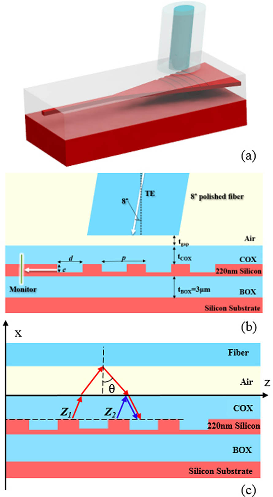
Figure 1(a) shows the proposed GC efficiency enhancement scheme by an 8° tilted and 8° polished APF. The cross-sectional schematic of the coupling system is shown in Fig. 1(b). From bottom to top, there are the silicon substrate, buried oxide layer (BOX), grating layer on 220 nm silicon, COX, air, and fiber, where the GC’s parameters are , , and . The layers’ interfaces in the chip are smooth through the chemical–mechanical polishing (CMP) processes in the conventional fabrication flow. The APF is available in the fiber-optics market.

Figure 1.(a) Proposed GC efficiency enhancing scheme with an 8° polished APF with its facet parallel to the chip surface. (b) Cross-sectional schematic of the 2D-FDTD model of a GC coupling with an 8° tilted APF. (c) Schematic of the light interferences in the air gap layer.
As is illustrated in Fig. 1(c), if we simplify the GC diffracted light into the plane wave and only analyze the interference in the air gap, the light emitted at and reflected at the upper surface will interfere with the light emitted at , which reflects at the lower surface. It is evident that the CE can be maximized when destructive interference happens in the air gap with proper thickness ().
The interference in COX is similar to that in an air gap, but the combined interference in both layers is much more complicated. Also, the GC diffracted light is far from a perfect plane wave, so it is much more convenient for us to study the combined enhancing influence on CE by the 2D-FDTD approach.
As shown in Fig. 1(b), a TE polarized fiber mode at 1565 nm is launched from the APF to the GC, and a monitor in the waveguide region will record the CE. Figure 2(a) illustrates the surface plot of the CE with various and . It is evident that the CE shows a periodic relation with both and . and have a combined influence on the total enhancing effect. The optimum around the maximum CE for different varies from 0.9 to , but the air gap enhancing effect is restricted by the directionality. The maximum CEs’ are always around , i.e., the corresponds to the maximum directionality. As the interference is not related to the GC structure, one can always find a proper to further improve the CE of a GC with an optimized .
Figure 2.(a) Surface plot for simulated CE with different and . (b) Simulated insertion loss of the GC with (blue) and (red) coupling with an APF (solid line) and a 12° tilted SMF (dashed line) with from 0.5 to . (c) Simulated transmission (solid line) and reflection (dashed line) spectra of APF (red) and 12° tilted SMF (blue) coupled GC with .
Figure 2(b) shows the CE changes periodically as increases from 0.5 to . is selected to be 1.84 and in order to simulate the maximum and minimum directionality cases. The maximum and minimum efficiency for is (59.0%) and (49.0%) with 1.14 and , respectively. Figure 2(b) also illustrates that the unparalleled fiber facet of a 12° tilted SMF causes a very weak interference in the air gap and consequently shows a small amplitude. The simulated CEs are about (52.9%) and (40.0%) for 1.84 and , respectively. These results suggest that the CE of this GC can be improved up to 1.69 dB by the combined effect of the interference in air gap and COX.
As interference is determined by the air gap and COX layers, this method can be applied to various GC structures. It is also noteworthy that is usually fixed to a certain range in experimental or packaging applications. An optimized is not universal for all kinds of GCs or even the same GC with different . For instance, though the CE of the GC with reaches its maximum when is , the CE of the GC with almost reaches its minimum at the same time. The improper for has decreased the CE for 2.6 dB, as shown in Fig. 2(b). If can be accurately operated, CE can be further improved by this method without any elaborate microstructures.
Figure 2(c) shows the transmission and reflection spectra of the GC with coupling with APF and SMF, respectively. The transmission at is evidently enhanced by the interference. The BW of the transmission spectrum is determined by the fiber angle offset loss and the interference effect in this work, as the GC structure as well as its diffraction efficiency spectrum remains unchanged. The fiber is usually fixed to a certain angle for the center wavelength. It is evident that the more the light deviates from the center wavelength, the more it deviates from the fiber angle, and also the more extra insertion loss there will be.
Though the incident angle at the fiber facet of 8° APF changes from SMF’s 0° to 12° at the center wavelength, the APF shows almost the same angle sensitivity, namely, wavelength sensitivity. The enhancing effect is slightly stronger at a long wavelength due to the selected and values. As a result, the 39.9 nm 1 dB BW of the APF case is slightly higher than the SMF case’s 37.8 nm, as plotted in Fig. 2(c).
Reflection of the APF case has a large decrease compared with the SMF case. The average back reflection of the APF case is within the 1 dB BW, while it is in the SMF case, as illustrated in Fig. 2(c). The interference enhancing effect causes a little fraction of reduction in back reflection, but the main reason is that the APF facet reflects the light into another direction other than reflecting it directly back into the GC as the SMF facet does.
The fiber angle and polishing angle’s effects on the CE have been also studied, where is selected to be . Figure 3(a) shows the air gap’s enhancing effects of APFs with different tilting angles from 6° to 10° with different relative polishing angles (defined as the actual polished angle minus the tilting angle). While the fiber facet is parallel to the COX surface, the CE can be improved by compared to SMFs’ at the same mode angle. The enhancing effect decreases as the relative polishing angle changes from 0° to 2°. It shows that the enhancing effect at a relative polishing angle is slightly better than that at 0°. The reason is that the analysis in Fig. 1(c) simplifies the GC mode as a plane wave. However, the actual GC diffracted mode is diverged, and the interference is consequently different from the plane wave case.
Figure 3.(a) Simulated enhancing effect of the air gap at different tilting and polishing angles. (b) Peak CE drops 0.15 dB as increases to .
Figure 2(a) seems to be a perfect periodic curve in a rather short range. However, as increases and becomes large enough, there will be a rather large fraction of light that has no chance to be interfered, and the amplitude of the efficiency curve will also decrease, as plotted in Fig. 3(b). The peaks of the curve also decrease 0.15 dB when increases from 0 to . It is evident that the APF should be as close as possible to the COX surface in order to achieve a higher enhancing effect. As the length of a fiber array along the axis is usually , a polished fiber facet could cause a and cancel out the merit of this polishing angle. By comprehensive consideration of both effects, the fiber facet should be parallel to the COX.
Figure 4(a) shows the simulated fiber alignment tolerance for both APF and SMF cases by varying the offset. The APF case shows a better offset tolerance. The offset 1 dB BWs are 6 and for the APF and SMF cases, respectively.
Figure 4.(a) Fiber alignment tolerance in the direction for the APF (red) and SMF (blue). (b) Enhancing effect by directionality only and various APF with different . (c) Maximum enhancing effect at various (red) and directionality’s 1.06 dB enhancing effect.
To experimentally examine the double layer interference enhancing effect, one can utilize the efficiency relation. It is difficult to accurately operate by a manual stage, but the fiber array can be raised up after being in contact with the die. The minimum movement resolution along the axis is , and the 0.02° fiber angular resolution could cause at most extra spacing for the fiber array. Accordingly, the minimum in the experiment should be .
Figure 4(b) shows that the directionality can be only improved by 1.06 dB by the COX interference. As the mode mismatch loss of the GC is not related to , the efficiency of a GC with the maximum directionality is 1.06 dB higher than that of the minimum. The maximum CE is improved by compared to the minimum when is fixed to . When is fixed to , the CE can only be improved by 1.05 dB, but the peak position changes into by the air gap interference. Though the submicron roughness of the fiber array facet could cause extra fiber spacing, the maximum enhancing effect still shows a good periodic relation with , as shown in Fig. 4(c). One can always find a proper to ensure that the maximum enhancing effect is larger than 1.06 dB with the directionality.
Based on the discussion above, an experiment was conducted to prove the double layer interference enhancing effect. The GC testing structure “GC loop” with initial COX shown in Fig. 5(a) was fabricated on an 8 ft SOI wafer in an external complementary metal–oxide–semiconductor (CMOS) foundry. The post-process on the die was carried out at the Collaborative Innovation Center of Advanced Microstructures of Nanjing University. We modified of the die by inductively coupled plasma reactive ion etching (ICP-RIE) and then tested its transmission. The COX thickness was measured at the same point in the middle of the loop to get the total silica thickness of the die (). A fiber array was used to measure the GC’s performance. The tilting angle of the fiber array with an 8° polished facet was fixed to 8°, and the measured center wavelength is 1565 nm. After the 12th measurement, the transmission already had its bottom, and thus the ICP-RIE process time and etching depth were increased to reduce the measurement times.
Figure 5.(a) Simulated (solid line) and measured (× mark) GC insertion loss with from 1.2 to coupling with an APF with . Inset: optical microscopy image of the “GC loop”. (b) Measured transmission spectra of the GC with COX coupling with SMF (blue) and APF (red).
The measured data matches quite well with the simulation, as plotted in Fig. 5(a). The measured maximum transmission is lower than the simulated because of the inevitable fabrication error. The measured maximum transmission is 1.71 dB larger than the minimum, which is very close to the curve’s 1.91 dB and is much higher than the directionality’s 1.06 dB. The measured curve is slightly distorted because we could not make absolutely sure of the same measurement conditions. The measured transmissions could fluctuate around the simulated curve, and the amplitude of the measured curve is consequently 0.2 dB lower than the simulated one. The measured curve and the simulated curve also show similar crest and trough positions.
Another GC with was fabricated to compare the transmission properties of the GC coupling with APF and SMF. Figure 5(b) illustrates that the measured transmission of such GC coupling with APF at 1565 nm is , which is higher than coupling with the SMF. It is evident that the APF’s spectrum has a better transmission at a longer wavelength and has a better 1 dB BW as well, which is consistent with the simulation results. This result also implies that properly designed and can simply improve CE without any extra microfabrication processes.
This method requires an APF facet and a flat chip surface. APFs are already widely used in many fiber-optic systems. Flat chip surfaces are commonly present due to the extensive use of CMP in microfabrications. In many cases, these polishing steps are already included in the fabrication processes and will not add extra cost. Note that an air gap is needed in this method so that index-matching epoxy cannot be used. Such epoxy is usually used to reduce reflection. Here, the use of an APF can help reduce reflection without such epoxy. The interference effect needed in this method requires accurate control of the air gap thickness during alignment. Note that in typical fiber–GC alignment, a stage with vertical position control is commonly used. Therefore, this method does not require additional equipment. However, the vertical alignment accuracy needs to be improved in this method compared to a normal fiber–GC alignment. This eventually becomes a cost-performance trade-off issue. Depending on various application scenarios, some cases may be willing to use this method to achieve lower loss while paying a bit more time in more precise alignment.
In conclusion, this Letter proposes a method to improve the GC’s efficiency simply by double layer interference without increasing complexity and expenditure in the microfabrication process. Simulation shows that CE can be improved by 1.6 dB by the combined interference of both the COX and air gap introduced by an APF with its polished facet parallel to the chip surface. The merits and restrictive factors in reflection, fiber alignment, and packaging/testing expenditure have also been discussed. The interference enhancing effect has finally been experimentally studied. This method provides an alternative approach to further improve different kinds of GCs’ CE.
References
[1] W. Song, R. Gatdula, S. Abbaslou, M. Lu, A. Stein, W. Y. Lai, J. Provine, R. F. W. Pease, D. N. Christodoulides, W. Jiang. Nat. Commun., 6, 7027(2015).
[2] N. Yang, H. Yang, H. Hu, R. Zhu, S. Chen, H. Zhang, W. Jiang. Photon. Res., 4, 233(2016).
[3] S. Cheung, T. Su, K. Okamoto, S. J. B. Yoo. IEEE J. Sel. Top. Quantum Electron., 20, 310(2014).
[4] H. Xu, X. Li, X. Xiao, P. Zhou, Z. Li, J. Yu, Y. Yu. Opt. Lett., 39, 4839(2014).
[5] H. Chen, P. Verheyen, P. D. Heyn, G. Lepage, J. D. Coster, S. Balakrishnan, P. Absil, W. Yao, L. Shen, G. Roelkens. Opt. Express, 24, 4622(2016).
[6] Z. Zhang, J. Hu, H. Chen, F. Li, L. Zhao, J. Gui, Q. Fang. Chin. Opt. Lett., 15, 041301(2017).
[7] M. Wang, L. Zhou, H. Zhu, Y. Zhou, Y. Zhong, J. Chen. Chin. Opt. Lett., 15, 042501(2017).
[8] X. Chen, C. Li, C. K. Y. Fung, S. M. G. Lo, H. K. Tsang. IEEE Photon. Technol. Lett., 22, 1156(2010).
[9] C. Zhang, J.-H. Sun, X. Xiao, W.-M. Sun, X.-J. Zhang, T. Chu, J.-Z. Yu, Y.-D. Yu. Chin. Phys. Lett., 30, 014207(2013).
[10] L. He, Y. Liu, C. Galland, A. E.-J. Lim, G.-Q. Lo, T. Baehr-Jones, M. Hochberg. IEEE Photon. Technol. Lett., 25, 1358(2013).
[11] R. Shi, H. Guan, A. Novack, M. Streshinsky. IEEE Photon. Technol. Lett., 26, 2158(2014).
[12] R. Marchetti, C. Lacava, A. Khokhar, I. Cristiani, D. Richardson, P. Petropoulos, P. MinzioniIntegrated Photonics Research, Silicon and Nanophotonics, ITu1A-2(2017).
[13] F. Van Laere, G. Roelkens, J. Schrauwen, D. Taillaert, P. Dumon, W. Bogaerts, D. Van Thourhout, R. Baets2006 Optical Fiber Communication Conference and the National Fiber Optic Engineers Conference, PDP15(2006).
[14] A. Mekis, S. Abdalla, D. Foltz, S. Gloeckner, S. Hovey, S. Jackson, Y. Liang, M. Mack, G. Masini, M. Peterson. IEEE Photonics Conference, TuQ2(2012).
[15] D. Vermeulen, S. Selvaraja, P. Verheyen, G. Lepage, W. Bogaerts, P. Absil, D. Van Thourhout, G. Roelkens. Opt. Express, 18, 18278(2010).