• Photonics Research
  • Vol. 10, Issue 9, B7 (2022)
Yu Li1、2, Xinhao Fan1, Xuyue Guo1, Yi Zhang3, Sheng Liu1, Bingyan Wei1, Dandan Wen1, Peng Li1、4、*, and Jianlin Zhao1、5、*
Author Affiliations
  • 1MOE Key Laboratory of Material Physics and Chemistry under Extraordinary Conditions, and Shaanxi Key Laboratory of Optical Information Technology, School of Physical Science and Technology, Northwestern Polytechnical University, Xi’an 710129, China
  • 2Xi’an Ming De Institute of Technology, Xi’an 710124, China
  • 3Department of Electronics and Nanoengineering, Aalto University, Espoo 02150, Finland
  • 4e-mail: pengli@nwpu.edu.cn
  • 5e-mail: jlzhao@nwpu.edu.cn
  • show less
    DOI: 10.1364/PRJ.463041 Cite this Article Set citation alerts
    Yu Li, Xinhao Fan, Xuyue Guo, Yi Zhang, Sheng Liu, Bingyan Wei, Dandan Wen, Peng Li, Jianlin Zhao. Metasurface for oscillatory spin splitting along the optical path[J]. Photonics Research, 2022, 10(9): B7 Copy Citation Text show less
    Illustration of metasurface interferometer for oscillatory spin splitting of light. (a) Sketch of the dielectric metasurface with two coaxial channels. (b) Schematic of RCP and LCP transforming and guiding via the metasurface with distinct modulation phases. C1 and C2 depict two pathways. Inset (upper): interferograms at a transverse plane for two spin states. Inset (below): spin angular momentum distribution in the r−z plane near the optical axis. (c) Illustration of the PB phases arising from photonic spin state transitions taken on the Poincaré sphere. The incident beam with RCP (denoted by |ψ+⟩) interacts with the meta-atom characterized as a half-wave plate by the rotation angle θ, leading to the output LCP (denoted by |ψ−⟩) state with PB phase denoted as 2θ and propagation phase ϕ0. (d) Illustration of the analogous AB effect. A and B are the locations of photonic spin state transition and interference, respectively. ϕC1 and ϕC1 depict the accumulated phases in two arms. ϕ±=ϕ0+ϕPB± are the concomitant phases corresponding to spin state transition.
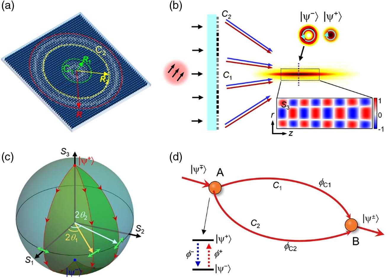
    Fig. 1. Illustration of metasurface interferometer for oscillatory spin splitting of light. (a) Sketch of the dielectric metasurface with two coaxial channels. (b) Schematic of RCP and LCP transforming and guiding via the metasurface with distinct modulation phases. C1 and C2 depict two pathways. Inset (upper): interferograms at a transverse plane for two spin states. Inset (below): spin angular momentum distribution in the rz plane near the optical axis. (c) Illustration of the PB phases arising from photonic spin state transitions taken on the Poincaré sphere. The incident beam with RCP (denoted by |ψ+) interacts with the meta-atom characterized as a half-wave plate by the rotation angle θ, leading to the output LCP (denoted by |ψ) state with PB phase denoted as 2θ and propagation phase ϕ0. (d) Illustration of the analogous AB effect. A and B are the locations of photonic spin state transition and interference, respectively. ϕC1 and ϕC1 depict the accumulated phases in two arms. ϕ±=ϕ0+ϕPB± are the concomitant phases corresponding to spin state transition.
    Design of the metasurface. (a) Wave vectors of fields in two pathways in the momentum space. (b) Modulation phases ϕ± and transmission requirement for designing the metasurface. (c) Schematic illustration of an element consisting of a Poly-Si nanopillar and a glass substrate. The geometric parameters of the element are denoted as H (height), L (length), W (width), and P (period), and the rotation angle is denoted as θ. (d) Transmission amplitude of nanopillar versus geometry parameters. These 16 black circles depict the parameters of these selected geometries, which work as half-wave plates with uniform transmittance. The white circle corresponds to the nanopillar with near-zero transmission amplitude selected to fill the opaque areas of the metasurface. (e) Transmission phases of the x-polarized eigenstate, phase retardations, and transmission amplitudes of two eigenstates of these selected nanopillars. (f) Simulated magnetic energy density distributions of an element with periodic boundary conditions, when x- and y-polarized lights (denoted as the red arrow and cross) illuminate the element. The black lines represent boundaries of the Poly-Si nanopillar (198 mm×196 mm×570 nm).
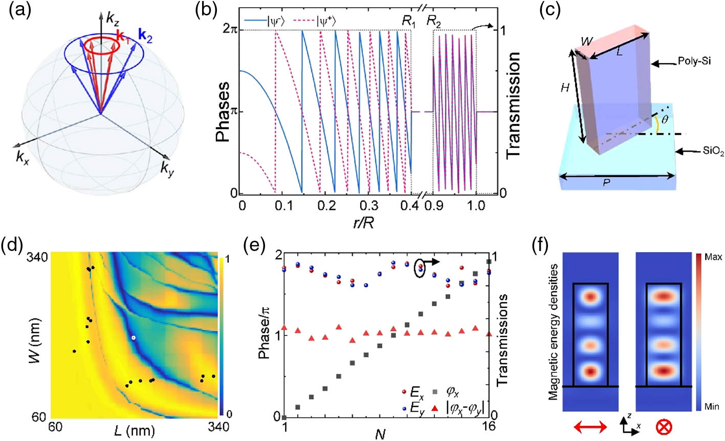
    Fig. 2. Design of the metasurface. (a) Wave vectors of fields in two pathways in the momentum space. (b) Modulation phases ϕ± and transmission requirement for designing the metasurface. (c) Schematic illustration of an element consisting of a Poly-Si nanopillar and a glass substrate. The geometric parameters of the element are denoted as H (height), L (length), W (width), and P (period), and the rotation angle is denoted as θ. (d) Transmission amplitude of nanopillar versus geometry parameters. These 16 black circles depict the parameters of these selected geometries, which work as half-wave plates with uniform transmittance. The white circle corresponds to the nanopillar with near-zero transmission amplitude selected to fill the opaque areas of the metasurface. (e) Transmission phases of the x-polarized eigenstate, phase retardations, and transmission amplitudes of two eigenstates of these selected nanopillars. (f) Simulated magnetic energy density distributions of an element with periodic boundary conditions, when x- and y-polarized lights (denoted as the red arrow and cross) illuminate the element. The black lines represent boundaries of the Poly-Si nanopillar (198  mm×196  mm×570  nm).
    Sketch of experimental setup. (a) Optical and (b) scanning electron microscope images of the metasurface and its local structure. The sample is composed of 3200×3200 elements with a lattice constant of 400 nm along the x and y axes. (c) Sketch of experimental setup. HWP, half-wave plate; QWP, quarter-wave plate; P, linear polarizer. The metasurface is placed on a linear translation stage to implement the z scan. Inset: scanning electron microscope images of local structures in two channels. The scale bar is 1 μm.
    Fig. 3. Sketch of experimental setup. (a) Optical and (b) scanning electron microscope images of the metasurface and its local structure. The sample is composed of 3200×3200 elements with a lattice constant of 400 nm along the x and y axes. (c) Sketch of experimental setup. HWP, half-wave plate; QWP, quarter-wave plate; P, linear polarizer. The metasurface is placed on a linear translation stage to implement the z scan. Inset: scanning electron microscope images of local structures in two channels. The scale bar is 1 μm.
    Observation of oscillatory spin splitting of light along the optical path. (a) Measured 3D intensity distribution of the focal field for the incidence of a linearly polarized field. The red dashed lines depict the z1=−20 μm and z2=60 μm planes. (b) Measured intensity distributions of the |ψ+⟩ and |ψ−⟩ states at the z1 and z2 planes. (c) Variations of Stokes parameter S3 (slices) in a longitudinal interval of about two periods. The S3 value depicts the density of spin angular momentum.
    Fig. 4. Observation of oscillatory spin splitting of light along the optical path. (a) Measured 3D intensity distribution of the focal field for the incidence of a linearly polarized field. The red dashed lines depict the z1=20  μm and z2=60  μm planes. (b) Measured intensity distributions of the |ψ+ and |ψ states at the z1 and z2 planes. (c) Variations of Stokes parameter S3 (slices) in a longitudinal interval of about two periods. The S3 value depicts the density of spin angular momentum.
    Measured on-axis Stokes parameter S3 when linearly polarized light beams with different polarization orientations illuminate two metasurfaces (I and II).
    Fig. 5. Measured on-axis Stokes parameter S3 when linearly polarized light beams with different polarization orientations illuminate two metasurfaces (I and II).
    Yu Li, Xinhao Fan, Xuyue Guo, Yi Zhang, Sheng Liu, Bingyan Wei, Dandan Wen, Peng Li, Jianlin Zhao. Metasurface for oscillatory spin splitting along the optical path[J]. Photonics Research, 2022, 10(9): B7
    Download Citation