Gallium nitride (GaN)-based light-emitting diodes (LEDs) are important for lighting and display applications. In this paper, we demonstrate green-emission (512 nm) InGaN quantum dot (QD) LEDs grown on a c-plane sapphire substrate by metal-organic chemical vapor deposition. A radiative lifetime of 707 ps for the uniform InGaN self-assembled QDs is obtained by time-resolved photoluminescence measurement at 18 K. The screening of the built-in fields in the QDs effectively improves the performance of QD LEDs. These high quantum efficiency and high temperature stability green QD LEDs are able to operate with negligible efficiency droop and with current density up to . Our results show that InGaN QDs may be a viable option as the active medium for stable LEDs.
1. INTRODUCTION
To date, commercial white light-emitting diodes (LEDs) are widely available using blue GaN LEDs to pump yellow phosphors [1]. However, GaN-based LEDs still suffer from a sublinear light output power (LOP) increase under high injection current, which is known as “efficiency droop” [2,3]. The origin of this droop phenomenon has been under intensive debate for over a decade, being attributed to many factors, including built-in fields [4], Auger recombination [5], and electron leakage [6]. Generally, III-nitride semiconductors grown along the crystallographic -axis encounter large built-in fields. Two contributors to the built-in fields are the spontaneous and piezoelectric polarization fields [7], with the latter being dominant due to the large lattice mismatch between InN and GaN. As a result, green InGaN LEDs, with high indium content, have a more severe drop in efficiency compared with blue ones [8]. The built-in fields in the InGaN/GaN active layer reduce the overlap between the electron and hole wave functions, and thus result in a reduced radiative recombination rate [9], leading to a strong efficiency droop [10].
LEDs utilizing InGaN quantum dots (QDs) in the active layer have been predicted to exhibit superior characteristics, including reduced efficiency droop, improved quantum efficiency, and temperature stability. Recently, both theoretical and experimental research has suggested that c-plane InGaN QDs can effectively reduce built-in fields [11,12]. The most common method of QD growth is self-assembly epitaxy in the Stranski–Krastanov (SK) mode. Currently, self-assembled InGaN QDs have been realized by both molecular beam epitaxy and metal-organic chemical vapor deposition (MOCVD) in the SK growth mode [13–15]. It should be noted that the InGaN QDs grown by this method always show a typical truncated pyramidal or disk-like shape. InGaN QDs with a base width larger than 50 nm grown by this method have resulted in LEDs with an external quantum efficiency (EQE) peak at a current density of [16]. The quasi-three-dimensional quantum confinement in these InGaN QDs is primarily provided in the longitudinal direction. More importantly, these QD structures are superior in the lateral carrier confinement by suppressing the non-radiative recombination loss through confining the carriers and preventing them from moving to nearby dislocations [17]. Furthermore, InGaN QDs inherently contain a lower density of structural defects and are more immune to the dislocations originating from the substrate [16,18]. However, the uniformity of QDs grown in the SK mode is difficult to control, and depends critically on the growth conditions. The inhomogeneous size distribution and varying indium composition in each QD can lead to bimodal height distribution of QDs [19], broadened photoluminescence (PL) spectrum [20], and long decay lifetimes in the biexponential function [21].
In this work, we report a green-emitting InGaN QD LED structure grown on a 2 in. c-plane sapphire substrate by MOCVD. Highly uniform InGaN QDs were achieved with unimodal height distribution, excellent short mono-exponential decay time, and reduced built-in fields. InGaN QD LEDs were then fabricated and characterized, showing high temperature stability, good internal quantum efficiency (IQE), and reduced efficiency droop.
Sign up for Photonics Research TOC. Get the latest issue of Photonics Research delivered right to you!Sign up now
2. MATERIAL GROWTH AND CHARACTERIZATION
Wafer bowing due to the large lattice constant and thermal expansion coefficient mismatch between GaN and the sapphire substrate is detrimental to uniform QD growth. The wafer becomes considerably concave when heated up to the high temperature for GaN growth. The heat transport from the substrate holder to the wafer becomes inhomogeneous due to the wafer bowing. In-incorporation is strongly dependent on temperature and thus results in substantial inhomogeneity of the QDs. Therefore, curvature management of the wafer bowing has a strong effect on the QD LEDs performance.
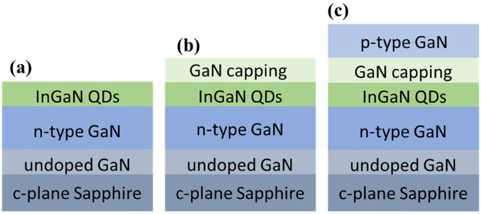
The epitaxial layers were grown using an Aixtron in. close coupled showerhead MOCVD system. Trimethylgallium, trimethylindium, and ammonia were employed as sources for Ga, In, and N, respectively, and 2 in. c-plane sapphire substrates were used. Before material growth, oxide desorption of the sapphire substrates was performed at 1000°C for 5 min. To achieve high-quality GaN with low dislocation density on a sapphire substrate, a low-temperature GaN nucleation layer followed by an undoped GaN layer is necessary. A 3 μm silicon-doped n-type GaN layer grown at 1050°C was optimized for smooth surface and lead to no bowing at the QD growth temperature. It is well known that the InGaN can only grow at temperatures much lower than that of GaN material. During the cooling process from GaN to InGaN, the concave bow of the wafer was flattened or even changed to convex. Equipped with an in situ temperature and curvature monitoring system (LayTec EpiTT) in the MOCVD system, the flat n-GaN layer with zero bowing was achieved by careful control of the cooling process. We believe this curvature engineering strategy minimized non-uniformities in size and indium composition for the InGaN QD. InGaN QDs were grown at 670°C with a V/III ratio of . Three samples were grown to characterize the QDs and QD LEDs. Figure 1(a) shows the InGaN QDs without capping, which were immediately cooled down to room temperature after the growth. It should be noted that to realize a QD LED structure, a GaN capping layer is necessary to protect the QDs during the subsequent high-temperature GaN growth. The QDs with a GaN capping structure are shown in Fig. 1(b). Figure 1(c) shows the QD LED structure, which was formed by an 80 nm thick magnesium-doped p-type GaN top layer grown at 880°C.
Figure 1.(a)–(c) Schematic structures of the InGaN QDs without capping, capped InGaN QDs, and InGaN QD LEDs.
After epilayer growth, X-ray reflectivity measurements were used to estimate the thickness of the InGaN QDs. For capped QDs, the distinct fringes that arise from the interfaces of two consecutive layers of GaN/InGaN/GaN heterostructure are clearly shown in Fig. 2(a). The 2.2 nm thickness of InGaN QDs for both QDs with and without capping was obtained by fitting. The (0002) omega-2theta scan curves of QD LEDs are shown in Fig. 2(b). The satellite peaks suggest that abrupt InGaN QD/GaN interfaces are formed. The indium composition and thickness of InGaN QDs are fitted to be 23% and 2.3 nm, respectively.
Figure 2.(a) X-ray reflectivity of QDs with and without capping; (b) omega-2theta scan curve of the QD LEDs.
The InGaN QD samples without capping were used to investigate the morphology of the QDs. As shown in the atomic force microscopy (AFM) image in Fig. 3(a), uniformly distributed QDs were obtained with a surface density and an average diameter of approximately and 66 nm, respectively. The height distribution is centered at 2.5 nm with a full width at half-maximum (FWHM) of 0.9 nm [Fig. 3(b)], indicating a relatively small dot inhomogeneity. Moreover, a unimodal Gaussian distribution of the QD heights suggests a homogeneous distribution of the QDs in size. Figure 3(c) shows the QD LEDs with a smooth surface.
Figure 3.(a) AFM image of InGaN QDs; (b) height distribution of InGaN QDs extracted from the AFM image; (c) AFM image of QD LEDs; (d) TRPL measurements of capped QDs.
The capped QD samples were used to investigate the carrier dynamics of the QDs by time-resolved photoluminescence (TRPL) measurements. TRPL measurements were performed at room temperature and 18 K using a Hamamatsu streak camera (temporal resolution: 2 ps) with a femtosecond pulsed laser (wavelength: 266 nm, repetition rate: 76 MHz, pulse width: 200 fs) as the excitation source of the photon density lower than the QDs density. Figure 3(c) shows the mono-exponential decay spectrum of the capped QDs at 300 K and 18 K. The lifetime is achieved as 480 ps at 300 K. The radiative lifetime is 707 ps assuming that the non-radiative recombination is completely suppressed at 18 K. The mono-exponential decay suggests size and indium composition uniformity of the QDs, which is consistent with the Gaussian height distribution revealed by AFM. It should be pointed out that the radiative lifetime is inversely proportional to the overlap of the electron and hole wave functions [22]. It is a big improvement compared with larger than 4 ns radiative lifetimes of green InGaN/GaN quantum well (QW) LEDs [23]. This shorter lifetime is strong evidence of the reduction of the built-in fields, and is even comparable with that of QDs grown along non-polar orientations [24].
A cross-sectional transmission electron microscope (TEM) image of the capped QDs taken along the GaN [110] direction is shown in Figs. 4(a)–4(c). QD diameter and spacing between the QDs range from 60–75 nm and 38–60 nm, respectively. This indicates that the diameters and density of the QDs agree well with the AFM results. The spacing between two neighboring QDs is clearly observed from Fig. 4(b). The high-magnification TEM image of the QDs shows their typical truncated pyramidal shape [Fig. 3(c)]. The high-resolution scanning transmission electron microscope (STEM) image in Fig. 4(d) shows a coherent and sharp GaN/InGaN QD interface without misfit dislocations, suggesting an elastically strained heterostructure. It can be concluded that the three-dimensional QD formation is due to the initially high-strained two-dimensional InGaN layers relaxing. Considering the slight difference in the spacing between QDs, it can be concluded that the QDs are approximately fully relaxed. The height of the QDs is about 2.3 nm, lower than that measured by AFM, possibly due to the curvature of the AFM tips.
Figure 4.(a) Cross-sectional TEM image of InGaN QDs sample with GaN capping layer; (b) high-magnification TEM image of the space between two neighboring QDs; (c) enlarged view of an InGaN QD; (d) STEM image of the interface between the InGaN QDs and GaN.
To investigate the influence of p-type GaN on the optical properties of the InGaN QDs, we compare the capped QDs (with 16 nm GaN-cap) and the QD LED using temperature-dependent photoluminescence (TDPL) from 10 K to 300 K, as shown in the TDPL spectra in Figs. 5(a) and 5(b).Figure 5(c) presents the TDPL peak energy for the capped QDs and LED, which shows an S-shaped shift with increasing temperature. This S-shaped behavior has been reported for the localization effect in both InGaN QDs and QWs [21,25,26]. At very low temperature (10 K), the mobility of photogenerated carriers is too small to reach the potential minima of the localization energy. As temperature increases, a red shift of the PL peak happens due to the carriers starting to recombine in the deeper localization potential. It is well known that the localization effect is due to the non-uniformity of QD diameters or alloy composition. Therefore, the comparatively smaller redshift of the LED indicates the QDs in it are more uniform than the capped QDs. As the temperature further increases, some of the carriers, with increased thermal energy, escape from the localization potential and induce a blueshift. The temperature of the turning point from redshift to blueshift for the QD LED () is found to be much lower than for the capped QDs (), which means the confinement energy of the localization states in the LED is comparatively smaller than that of the capped QDs. In order to further clarify the TDPL peak energy, Varshni’s empirical formula is considered: where is the bandgap energy at , and are Varshni’s thermal coefficients, is the standard deviation in the energy distribution width of the localized states indicating the degree of the localization effect, and kB is the Boltzmann constant. The solid lines in Fig. 5(c) are the fitting curves according to Varshni’s formula, where is obtained to be 31 and 24 meV for the capped QDs and LED, respectively. The small value of in the LED is attributed to the high-temperature p-GaN growth enhancing the interface and improving the uniformity of the QDs. This effect also induces a redshift of the LED compared to capped QDs. Therefore, the peak wavelength of the LED is quite stable with temperature at 512 nm (2.42 eV), indicating that uniform QDs offer much better thermal stability for LEDs. The PL FWHM of these two samples shows a similar trend, implying that the p-GaN layer growth results in an equally strong confinement effect of the carriers in the QDs.
Figure 5.TDPL spectra of (a) QD with capping and (b) QD LED; (c) PL peak energy; and (d) PL FWHM of InGaN QD with capping and QD LED.
First, the wafers were pre-cleaned in sulfuric acid/hydrogen peroxide (H2SO4:H2O2=5:1) and aqua regia solution (HCl:HNO3=3:1) for 5 and 10 min respectively, followed by four cycles of de-ionized water rinsing in wet-station. Mesa isolation was then patterned by standard photolithography using a Karl Suss MA-6 photo-aligner. Inductively coupled plasma etching was used to etch down to the n-type GaN. In this study, the semitransparent Ni/Au (50/50 Å, 1 Å = 0.1 nm) was used as current spreading layer to achieve lower forward voltage. Cr/Al/Ti/Au (100/1000/500/500 Å) was deposited as the n-electrode and automatically formed ohmic contact on n-GaN. Finally, the epilayer was diced into isolated devices with .
4. CHARACTERIZATION OF DEVICES
Figures 6(a) and 6(b) show the forward voltage and LOP, respectively, as a function of injection current density. The LOP increases linearly with the increase of the injected current density up to . To investigate the built-in fields in the QDs, the electroluminescence (EL) spectra of the LED under various injection current densities at room temperature are shown in Fig. 6(c). It is well known that the EL wavelength shift with increasing current injection is an important sign for observation of built-in fields [27]. As the injection current density is gradually increased from to , the peak wavelength of the QD LED located at 512 nm (2.42 eV) exhibits no shift, and is practically the same as the PL wavelength, implying fully screened built-in fields. Although an EL emission peak wavelength with a negligible shift has already been reported for green c-plane InGaN QDs and green semipolar InGaN QW LEDs [11,27], green QD LEDs without an observable efficiency droop have yet to be reported. The EQE as a function of the injection current density is depicted in Fig. 6(d). The efficiency without droop up to an injection current density of is owing to the fully screened built-in fields inducing an increase in the radiative recombination rate. The variation of the IQE with current density can be calculated by using the following relations: and , where , and are the injected carrier density, QD height of 2.3 nm, Shockley–Read–Hall coefficient, the radiative recombination coefficient, and the Auger recombination coefficient, respectively. , , and are obtained as , , and , respectively. The Auger recombination coefficient of this QD LED is comparable with blue LEDs grown on a free-standing GaN substrate [28], indicating that Auger recombination does not contribute to efficiency droop. It has been reported that the PL intensity increases drastically as the number of stacked InGaN QD layers increases [29]. A future study of homogeneous InGaN QD stacks with further optimization of the growth conditions is planned to improve the performance of QD LEDs.
Figure 6.(a) Forward voltage versus injection current density; (b) LOP versus injection current density; (c) electroluminescence spectra of QD LED; (d) EQE as a function of current density.
In summary, uniformly distributed c-plane InGaN QDs with a short lifetime are obtained. A c-plane InGaN self-assembled QD LED emitting at 512 nm is realized with decent quantum efficiency, high wavelength stability, and high thermal stability, which represents a major step toward high-efficiency GaN-based LEDs. The QD LED shows a stable EL emission wavelength and sustained EQE at high injection current density up to . This is strong evidence that InGaN QDs with fully screened built-in fields can significantly improve LED performance and solve the efficiency droop problem. Our demonstration opens a new pathway to solving the efficiency droop and green gap problems of GaN-based LEDs.
Acknowledgment
Acknowledgment. The authors would like to thank the MCPF and NFF of HKUST for technical support.