Abstract
As the key part of chip-scale atomic clocks (CSACs), the vapor cell directly determines the volume, stability, and power consumption of the CSAC. The reduction of the power consumption and CSAC volumes demands the manufacture of corresponding vapor cells. This overview presents the research development of vapor cells of the past few years and analyzes the shortages of the current preparation technology. By comparing several different vapor cell preparation methods, we successfully realized the micro-fabrication of vapor cells using anodic bonding and deep silicon etching. This cell fabrication method is simple and effective in avoiding weak bonding strengths caused by alkali metal volatilization during anodic bonding under high temperatures. Finally, the vapor cell D2 line was characterized via optical-absorption resonance. According to the results, the proposed method is suitable for CSAC.With the developments of quantum engineering technology and micro-/nano-processing, micro-system, micro-miniature, ultra-low power, and chip-level system integrations have become the tendency of quantum instruments, such as atom interferometer magnetometers, atomic clocks, and atomic gyroscopes[1,2]. Over the past decades, much attention has been devoted to the development of miniaturized atomic clocks. An atomic clock is based on coherent population trapping (CPT) without a microwave cavity. The future goal of atomic-clock miniaturization is the realization of chip-scale atomic clocks (CSAC)[3,4]. As the most important component of CPT clocks, the vapor cell directly determines the volume, stability, and power consumption of the atomic clock[5]. Hence, the vapor cell is the key component for atomic-clock miniaturization[6,7]. With the reductions of power consumption and atomic-clock volumes, suitable vapor cells must be designed.
The traditional atomic vapor cell preparation mainly adopts glass-blowing and cylindrical vapor cells made from hollow-core glass fibers with lasers. This procedure can realize the miniaturization of atomic vapor cells to a certain extent[8,9]. However, this method typically leaves a sealed glass stem protruding from the cell, which makes the assembly of the cell with other optical components difficult. In addition, the glass easily reacts with alkali metal atoms at high temperatures and creates large amounts of residue, which is unsuitable for microelectromechanical system (MEMS) cells[10,11]. Therefore, those techniques cannot be applied for CSACs.
The MEMS technology provides a simple way to miniaturize atomic vapor cells and increases their potential for mass production[12–15]. Because of the strong reactivity of alkali metals, they must be kept in an inert atmosphere and stored in hermetically sealed containers or under an inert liquid. Based on the different filling technologies of alkali metals, the fabrication methods for vapor cells can be classified into five groups: (1) in-situ chemical-reaction method[16,17]; (2) deposition of alkali metal azides via UV decomposition[18]; (3) direct alkali metal-filling techniques[19]; (4) laser ablation of encapsulated alkali metals in wax micro-packet[20]; (5) electrolytic decomposition of alkali metal-enriched glass[21].
Sign up for Chinese Optics Letters TOC. Get the latest issue of Chinese Optics Letters delivered right to you!Sign up now
The in-situ chemical-reaction method is one of the simplest methods of all vapor cell preparation technologies. However, the method generates impurities that remain in the cavity and cause frequency drifts resulting in insufficient long-term spectral line drifts[22]. The deposition of alkali metal azides via UV decomposition is a cost-effective solution and enables the batch preparation of vapor cells[23]. However, since the alkali metal quantity is directly limited by the buffer gas pressure, reactions of alkali metal with impurities inside the cell and cell wall must be limited[24]. Direct alkali metal-filling techniques provide pure alkali metals inside the cell and avoid interferences with impurities inside the cell. However, an alkali metal easily oxidizes in an atmospheric environment, which implies that the fabrication should be performed under vacuum and must be adapted to or designed for this technique[25]. The electrolytic decomposition of alkali metal-enriched glass can control the filling amounts of alkali metal elements and realize a wafer-level batch manufacture. However, this method exhibits a higher operation complexity than the others and causes more costs. In addition, different currents will produce different results. The laser ablation of encapsulated alkali metals in the wax micro-packet production is extremely complex and unsuitable for batch production. Hence, it has not been widely adopted[26]. In addition, in most techniques, it is necessary to bond glass and silicon substrates to seal the alkali metal. However, the bonding process is usually carried out at temperatures above the melting point of the alkali metal. This leads to the vaporization of the alkali metal, which then adheres to the surface of the bonded silicon wafer and affects the bonding strength. Therefore, the most challenging part of the cell fabrication comprises the deposition of the alkali metal into the cell and the subsequent sealing.
In this Letter, we present a set of simple and feasible technical solutions for the preparation of vapor cells. The vapor cell is designed with two cavities, the smaller of which is used as reaction chamber, and the larger one is employed as an optical cavity. To solve the problem of the weak bonding strength due to the alkali metal volatilization during anodic bonding under high temperatures, we use a rubidium (Rb) dispenser ( and Zr–Al alloy mixture) from SAES Getters, which remains stable at an anodic-bonding temperature of 500°C. After the anodic-bonding process is completed, the Rb dispenser is activated and releases Rb vapors via a titanium sapphire laser. The optical-absorption resonance of the natural Rb D2 line in the vapor cell is detected through experimental tests. According to the results, the fabrication of the Rb vapor cell was successful.
The first condition for the selection of the anodic-bonding material is whether the thermal-expansion coefficients of the two materials match. Otherwise, the bonding surface might crack or break, owing to thermal stress generated during the high-temperature anodic-bonding process[27]. In this experiment, a 4 in. P-type double-sided polished silicon wafer with crystal direction and a thickness of 1.5 mm is prepared. The high-temperature-resistant glass with a thickness of 500 μm is employed. Its thermal-expansion coefficient is very close to that of the silicon wafer. To obtain a good bonding strength, both glass and silicon wafers are required to have a good surface roughness and flatness.
Because alkali metals are relatively chemically active materials that react easily with oxygen and water vapor in the air, the key step of the micro-atomic vapor cell fabrication is the filling of alkali metal atoms into the cells[28]. The employed Rb dispenser (alkali metal chromate with Zr–Al alloy employed as a reducing agent) from SAES Getters exhibits a high stability at up to 500°C in bonding processes and can only release Rb vapor at high-power laser heating temperatures of above 700°C after vapor cell sealing. This process does not cause any damages to the silicon–glass surface or bonding quality. The alkali metal is generated via a chemical reaction between the chromate and Zr–Al alloy ()[29]:
The product contains only one gas component: Rb. The other components are oxides with stable chemical properties.
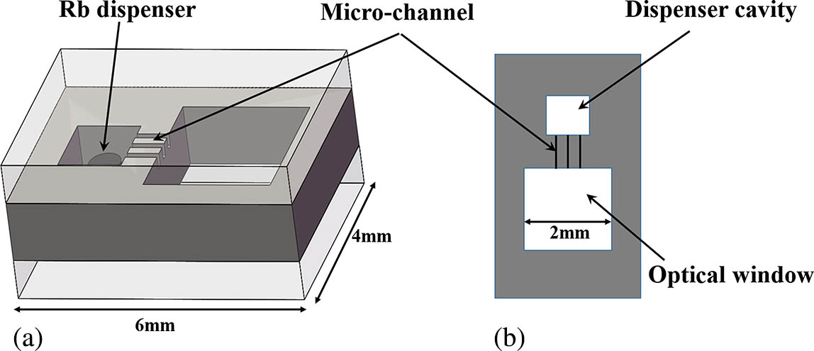
Figure 1 shows the schematic structure of the vapor cell, which is composed of two cavities. The smaller cavity is the reservoir with the Rb dispenser. The bigger cavity is filled with the alkali metal and used as an optical window. The two cavities are connected via three micro-channels to prevent impurities from entering the optical window of the vapor cell. The micro-channel has a height of 0.5 mm and a width of 0.2 mm. The size of the vapor cell is .

Figure 1.Structure of vapor cell: (a) 3D structure of vapor cell; (b) cross section of vapor cell.
The micro-fabrication steps for the atomic vapor cell are schematically shown in Fig. 2. A 4 in. P-type and 1.5 mm thick silicon wafer with crystal orientation is prepared.
Figure 2.Micro-fabrication steps of atomic vapor cell. DRIE, deep reactive ion etching.
In the step shown in Fig. 2(a), the silicon wafer is cleaned and dried according to the (RCA) standard to remove organic or inorganic contaminants. Then, spin coating with a thin layer of hexamethyldisilazane (HMDS) primer is employed. This step will ensure a strong adhesion of the photoresist to the substrate groups.
In the step shown in Fig. 2(b), a photoresist (AZ 4620) of constant thickness is spin-coated onto the front of the silicon wafer. Afterward, the sample is placed for 10 min into an oven to remove any excess solvent remaining in the photoresist and to reduce the stress inside the resist to increase the adhesion of the photoresist layer to the wafer.
In the step shown in Fig. 2(c), the silicon wafer is photolithographically patterned via UV light exposure through a glass plate as a photo mask. After the exposure, the silicon wafer is immersed into the positive developer AZ 4620 and shaken until the pattern is clearly visible. The sample is rinsed in water and dried. Then, it is placed into an oven for 30 min to remove the residual developer and anneal the photoresist layer, thereby enhancing the interfacial adhesion between the photoresist and wafer and further increasing the hardness of the photoresist, which is preferable for dry etching.
In the step shown in Fig. 2(d), the front is etched to a depth of approximately 800 μm. The complete process comprises a front and back etching to further improve the quality of the deep reactive ion etching (DRIE)-processed surface. Then, the silicon wafer is placed into an SLD 310 degumming solution and heated to 60°C for 30 min to remove the photoresist remaining on the silicon wafer surface.
In the step shown in Fig. 2(e), AZ 4620 photoresist is spin-coated onto the back of the silicon wafer.
In the step shown in Fig. 2(f), back etching and DRIE are conducted to achieve the final depth of the wafer structure.
In the step shown in Fig. 2(g), after the cell cavity etch is completed, the photoresist remaining on the silicon wafer surface is removed via the SLD 310 degumming solution. Next, a photoresist layer of approximately 5 μm is sprayed onto the front surface of the silicon wafer using a glue dispenser. The micro-channel structure is etched through DRIE.
In the step shown in Fig. 2(h), the etched wafer is anodic-bonded onto a 4 in. glass wafer at 500°C with the wafer bonder EVG510. Prior to the first anodic bonding, the glass wafer and etched silicon wafer are rinsed in an aqueous solution with a mixing ratio of of sulfuric acid and hydrogen peroxide and later rinsed with deionized water. Subsequently, the wafer is dry-blown with nitrogen and baked on a hot plate at 110°C to remove residual moisture. The anodic bonding of the glass and silicon wafers is carried out in a bonding vacuum chamber with less than pressure and at 450°C. The bonding voltage slowly rises from 200 to 1200 V and remains at 1200 V until the bonding current drops below 10% of the peak value. Then, the structure is cooled to room temperature to complete the first anodic-bonding process. Throughout the bonding process, a force of 1200 N is applied. The silicon–glass cavities after the first successful anodic-bonding process are schematically shown in Fig. 2(h).
In the step shown in Fig. 2(i), the Rb dispenser micro-pill is inserted into the silicon–glass cavities. The micro-pill has a cylindrical shape with a diameter of approximately 1 mm and a height of approximately 0.6 mm. Afterward, the bonding-chamber pressure is pumped down to approximately . Both wafers are heated up to 450°C and flushed with a buffer gas of up to 10 kPa. Subsequently, the silicon–glass cavities are sealed with a 500 μm thick glass wafer to create a sandwich structure, as shown in Fig. 2(j). The portion of the top heater is moved downward to provide a contact force of 1000 N on the sandwich structure, and the bonding voltage slowly rises from 200 to 1200 V. The total bonding process is completed after 20 min.
In the step shown in Fig. 2(k), alkali vapor evaporates from a small pill, owing to a high-power titanium sapphire laser with a wavelength of 852 nm and a spot size below 1 mm. The laser beam is focused on a small area of the dispenser to avoid damages to the glass and silicon wafers during excitation. The laser is operated at 2.5 W, and the Rb dispenser is exposed to the laser light for 3–5 min.
Figure 3(a) shows the three-dimensional (3D) schematic in silicon holes under a confocal microscope. Figure 3(b) shows the wafer with vapor cells before dicing. In Fig. 3(c), a scanning electron microscope (SEM) image of a single vapor cell wafer after etching is presented. Figure 3(d) shows an enlarged partial view of the micro-channel. In a cell, the left cavity is the dispenser cavity, and the right cavity is the optical window.
Figure 3.(a) 3D schematic of silicon pore structure; (b) wafer with vapor cells; (c) SEM image of DRIE of vapor cell; (d) enlarged partial view of micro-channel.
After the second anodic bonding, the silicon wafer is diced into many single cells with external dimensions of , as shown in Fig. 4.
Figure 4.Micro-fabricated vapor cell on top of a coin.
Optical-absorption measurements were performed to confirm the existence of Rb in the cells. Figure 5 presents the experimental setup. The cell is placed between two heated glass wafers made from indium tin oxide (ITO). The heating temperature is kept in a range of 50–100°C. The heater—fabricated by glass substrates with non-conductive epoxy resin—has a temperature precision of the order of 1 mK. To decrease the influence of the external magnetic field, the cell is surrounded by three nested cylindrical magnetic shields. A pair of Helmholtz coils sits between the shields and provides 5 μT along the light propagation direction.
Figure 5.Experimental setup for measurement of the optical-absorption spectrum. TLB, tunable laser; OI, optical isolator; PBS, polarizing beam splitter; NDF, neutral density filter; QWP, quarter-wave plate; M1, high-reflection mirror; PD, photodiode.
A tunable laser (TLB) from New Focus (diameter of 1 mm, central wavelength of 780 nm, line width below 300 kHz) is used as a light source. To prevent optical feedback, the laser beam passes through an optical isolator. A neutral density filter (NDF) is used to change the intensity of laser light. After passing through an NDF, the laser beam is divided into two beams through the polarizing beam splitter (PBS). One beam is used as input for the high-precision wavelength meter to verify the laser wavelength of approximately 780 nm. The other beam passes through the quarter-wave plate and obtains a circular polarization. Then, the laser beam passes through the vapor cell, which is heated to a controlled temperature ranging from 50°C to 100°C. The function generator generates a triangle wave of appropriate frequency and amplitude to scan the voltage across the piezoelectric transducer (PZT) inside the laser assembly and changes the laser frequency to obtain atomic-absorption lines. Hence, the photodiode (PD) behind the vapor cell can detect the optical-absorption spectrum, which is presented by an oscilloscope.
Figure 6 presents the D2 line absorption spectra for 50, 60, 70, 80, 90, and 100°C of the vapor cells that were measured after about two months. The spectra exhibit four distinct peaks. Each peak consists of three very close peaks, which are difficult to distinguish owing to Doppler broadening. The depth of each peak represents the relative abundance of an isotope in naturally occurring Rb. Naturally occurring Rb consists of 72.17% 85Rb and 27.83% 87Rb. Thus, the two signals with higher amplitudes are of 85Rb, whereas the outer two dips correspond to the absorption of 87Rb. Moreover, the amplitudes of the absorption peaks increase with increasing temperature, as expected for an increasing Rb vapor density.
Figure 6.D2 line absorption spectra of vapor cell.
In this study, the micro-fabrication of atomic vapor cells for CSACs was investigated by anodic bonding and deep silicon etching. The vapor cell was manufactured with a dual-cavity structure in an MEMS process. Further, a commercially available Rb dispenser from SAES Getters was inserted into the micro-cell and locally heated. This procedure overcomes overflow of alkali metals, which affects the bonding strength during anodic bonding. Moreover, the shortage of the optical path caused by chemical-reaction residue is avoided. The optical-absorption resonance of natural Rb could be detected in the vapor cell, which proves that the scheme is feasible for the preparation of atomic cells. In conclusion, the measurement results confirm the suitability of the proposed process for novel compact or miniaturized atomic devices such as atomic clocks, atomic magnetometers, and gyroscopes.
References
[1] J. Kitching. Appl. Phys. Rev., 5, 031302(2018).
[2] H. Dong, J. Fang, B. Zhou, J. Qin, S. Wan. Microsyst. Technol., 16, 1683(2010).
[3] P. Knapkiewicz. Micromachines, 9, 405(2018).
[4] R. C. Dong, J. D. Lin, R. Wei, W. L. Wang, F. Zou, Y. B. Du, T. T. Chen, Y. Z. Wang. Chin. Opt. Lett., 15, 050201(2017).
[5] S. L. Li, J. Xu, Z. Q. Zhang, L. B. Zhao, L. Long, Y. M. Wu. Chin. Phys. B, 23, 470(2014).
[6] R. Han, Z. You, F. Zhang, H. Xue, Y. Ruan. Micromachines, 9, 175(2018).
[7] X. T. Zhang, G. Q. Yang, K. Dai, Y. Chen. Chin. Opt. Lett., 15, 070201(2017).
[8] S. Knappe, V. Velichansky, H. G. Robinson, J. Kitching, L. Hollberg. Rev. Sci. Instrum., 74, 3142(2003).
[9] T. Rajesh, K. Kevin, F. Mohammed, N. Ahmer, O. L. Weaver, K. L. Corwin. Opt. Lett., 31, 2489(2006).
[10] E. J. Eklund, A. M. Shkel, S. Knappe, E. Donley, J. Kitching. IEEE International Conference on Micro Electro Mechanical Systems, 171(2008).
[11] W. Yang, D. B. Conkey, B. Wu, D. Yin, A. R. Hawkins, H. Schmidt. Nat. Photon., 1, 331(2007).
[12] S. Woetzel, V. Schultze, R. Ijsselsteijn, T. Schulz, S. Anders, R. Stolz, H. Meyer. Rev. Sci. Instrum., 82, 033111(2011).
[13] C. Gorecki. Procedia Eng., 47, 898(2012).
[14] P. Knapkiewicz, J. Dziuban, R. Walczak, L. Mauri, P. Dziuban, C. Gorecki. Procedia Eng., 5, 721(2010).
[15] S. Karlen, J. Gobet, T. Overstolz, J. Haesler, S. Lecomte. Opt. Express, 25, 2187(2017).
[16] S. Knappe, V. Gerginov, P. D. D. Schwindt, V. Shah, H. G. Robinson, L. Hollberg, J. Kitching. Opt. Lett., 30, 2351(2005).
[17] Y. Ji, J. Shang, Q. Gan, L. Wu. 2017 IEEE 67th Electronic Components and Technology Conference (ECTC), 136(2017).
[18] L. A. Liew, J. Moreland, V. Gerginov. Appl. Phys. Lett., 90, 114106(2007).
[19] L. A. Liew, S. Knappe, J. Moreland, H. Robinson, L. Hollberg, J. Kitching. Appl. Phys. Lett., 84, 2694(2004).
[20] S. Radhakrishnan, A. Lal. International Conference on Solid-state Sensors(2005).
[21] F. Gong, Y. Y. Jau, K. Jensen, W. Happer. International Frequency Control Symposium and Exposition, 3946(2006).
[22] J. Su, K. Deng, D. Z. Guo, Z. Wang, J. Chen, G. M. Zhang, X. Z. Chen. Chin. Phys. B, 19, 110701(2010).
[23] K. Tsujimoto, K. Ban, Y. Hirai, K. Sugano, T. Tsuchiya, N. Mizutani, O. Tabata. J. Micromech. Microeng., 23, 115003(2013).
[24] K. Ban, Y. Hirai, K. Tsujimoto, A. Terao, N. Mizutani, T. Kobayashi, O. Tabata. J. Vac. Sci. Technol. A: Vac. Surfaces Films, 34, 061601(2016).
[25] F. Vecchio, V. Venkatraman, H. R. Shea, T. Maeder, P. Ryser. Sens. Actuators A, 172, 330(2011).
[26] S. Chen, Y. Ruan, B. Ma. Key Eng. Mater., 562, 1361(2013).
[27] M. Hasegawa, R. K. Chutani, C. Gorecki, R. Boudot, P. Dziuban, V. Giordano, S. Clatot, L. Mauri. Sens. Actuators A, 167, 594(2011).
[28] J. Liu, J. Shang, J. Tang, Q. A. Huang. J. Microelectromech. Syst., 20, 909(2011).
[29] V. Maurice, J. Rutkowski, E. Kroemer, S. Bargiel, N. Passilly, R. Boudot, C. Gorecki, L. Mauri, M. Moraja. Appl. Phys. Lett., 110, 164103(2017).