Phase carried by two orthogonal polarizations can be manipulated independently by controlling both the geometric size and orientation of the dielectric nanopost. With this characteristic, we demonstrate a novel multifunctional metasurface, which converts part of the incident linearly polarized light into its cross-polarization and encodes the phase of the two orthogonal polarizations independently. A beam splitter and a bifocal metalens were realized in a single-layer dielectric metasurface by this approach. We fabricated the bifocal metalens and demonstrated that two focal spots in orthogonal polarizations can be separated transversely or longitudinally at will. The proposed approach shows a new route to design multifunctional metasurfaces with various applications in holography and three-dimensional display.
The metasurface[1–7] is an artificial planar structure consisting of subwavelength optical scatters that locally control the polarization, amplitude, and phase of light in reflection or transmission, which has extremely small volume, and has been applied to realize various optical functionalities such as wave plates[8], lenses[9], and holograms[10,11].
By integrating diverse functionalities into one single device, the multifunctional metasurface[12–14] is more efficient in miniaturization and integration and has broad applications in on-chip photonic circuits[15–17] and imaging processing[18,19]. An intuitive way to realize the multifunctional metasurface was to assemble two metasurfaces onto a single plane[20,21]. However, the efficiency was always low due to the interference between different functionalities. Afterwards, people tried to carefully design a birefringent meta-atom to encode more functionalities onto a single metasurface, which rely on the diverse optical response of the meta-atom depending on the polarization[22–28], wavelength[29], or incident angle[30,31]. Because of optical anisotropy of the meta-atom, different phase profiles can be encoded for two orthogonal polarizations along the optical axes in a single metasurface by changing the length and width of each nanopost[25,26]. If both the size and orientation of each nanopost are modified[12], both the propagation phase and geometric phase can be imposed to modulate the wavefront through the metasurface, and spatial phase profiles can be manipulated independently for arbitrary orthogonal polarizations. For instance, two dissimilar holograms[12], topological numbers[28], or metalenses[24] can be reconstructed from a single metasurface for left- and right-handed circular polarizations.
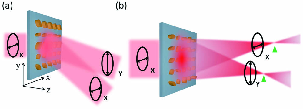
In this paper, we present a new strategy to independently control the phase of two orthogonal polarizations with an all-dielectric metasurface. Part of the linearly polarized incident light is converted into the cross-polarization and the phase of co- and cross-polarized light can be coded independently by modifying the geometric size and orientation of the elliptical nanopost. Unlike the function of the polarization beam splitter, which deflects two eigen polarizations to different directions, our designed metasurface splits the linearly polarized incident light into two output beams with co- or cross-polarization and propagation along different directions [Fig. 1(a)]. Thereafter, a bifocal metalens, which focuses linearly polarized incident light onto two different positions, is demonstrated [Fig. 1(b)], and the polarization of two focal spots is co- and cross-polarized to the incident polarization, respectively. Moreover, the proposed method provides an intuitive approach for three-dimensional (3D) display, which needs to record a pair of orthogonally polarized images from a same scene in different perspectives simultaneously to convey depth perception for binocular stereo vision, encoding two offset images for co-polarized and cross-polarized light, respectively. In general, this method will pave a new route to design multifunctional metasurfaces and have various applications in holography and multi-image systems.
Sign up for Chinese Optics Letters TOC. Get the latest issue of Chinese Optics Letters delivered right to you!Sign up now
Figure 1.Schematic illustrations of the multifunctional metasurface. (a) The designed metasurface splits the x-polarized incident light into two different directions. (b) The designed metalens focuses the x-polarized incident light on two independent focal spots.
2. Principle of Independent Phase Manipulation for Orthogonal Polarizations
Figure 2(a) presents the unit cell composed of the elliptical amorphous silicon (, ) cylinder on the quartz substrate, where the major ( axis) and the minor ( axis) lengths are and , respectively, the height of the cylinder is , and the period of the unit is . The elliptical cylinder is rotated by the angle for its major axis relative to the axis. For -polarized incident light, the electric field of incident light is decomposed into and along the axis and axis first [Fig. 2(b)] and interaction with the nanopost can be described by the complex amplitude transmittance along the axis () and axis (). The electric field of the output light is decomposed along the axis and axis again to obtain the complex amplitude transmittance of different polarizations and , which can be calculated as follows:
Figure 2.Optical response for elliptical cylinder at freespace wavelength of 633 nm. All of the phases are in units of rad/π. (a) Schematic of the Si elliptical cylinder located on the quartz with parameters P = 300 nm, H = 410 nm, Do and De. (b) Schematic of the meta-atom optical response. (c), (d) Phase and amplitude of as functions of Do and De. (e) Phase delay of as a function of Do and De. (f)–(h) Phase delay ϕxx as a function of the rotation angle α for different phase delays ϕyx, which are +0.55π, −0.55π, and ±π and marked with blue triangles, green squares, and red circles in (d) and (e), respectively.
It is noted that the phase delay of -polarized output light () is determined only by , and the phase delay of the co-polarized output light depends on both , and orientation angle . Figures 2(c) and 2(d) show the phase and amplitude of transmittance depending on and at a wavelength of 633 nm. Exchanging and , the plots of Figs. 2(c) and 2(d) will represent the phase and amplitude of , respectively. As shown in Fig. 2(e), the phase difference between and covers the entire range for various D from 60 nm to 220 nm at the wavelength of 633 nm. To elaborate the feasibility of independent phase manipulation on and , we choose an arbitrary phase delay [by the blue triangle, green square, and red circle, respectively, in Figs. 2(d) and 2(e)] and then calculate the phase delay of by rotating the nanopost from 0 to 90°. It is seen clearly that the phase delay can cover the range by only rotating the orientation angle for all of the arbitrary phase differences of [Figs. 2(f)–2(h)].
3. Simulation and Experimental Results of the Designed Metasurfaces
As a verification of independent phase manipulation for orthogonal polarizations, we designed a metasurface for splitting and deflecting the orthogonally polarized beams. As shown in Fig. 3(a), sixteen specific cells with different geometric sizes are arranged to constitute a supercell for the deflector. Under -polarized light illumination, the phase delays for -polarized components of the transmitted light are presented in Fig. 3(b), indicating that the phase delay of the -polarized output increases from 0 to in the step of , simultaneously, the phase delay of the -polarization output increases from 0 to in the step of [Fig. 3(c)]. The simulated optical transmissions for both - and -polarization are all around 40% [red triangles in Figs. 3(b) and 3(c)].
Figure 3.Simulation results of the metasurface for splitting and deflecting the orthogonal polarization beam. (a) The supercell consisting of sixteen specific nanoposts. (b), (c) The phase delay φxx and φyx and their corresponding transmission of selected sixteen cells. The black line is the theoretically requested phase delay. (d), (e) The electric field contributions of x-polarization and y-polarization in the x–z plane with x-polarized incident light.
The different deflections for - and -polarization components are further corroborated by the finite-difference time-domain (FDTD) simulations. Figures 3(d) and 3(e) depict the simulated electric field distributions of and , respectively, under normal incidence of -polarized light. It is seen that the output wavefront is tilted by a deflection angle of , and the wavefront has an oblique angle of , which is consistent with the theoretical prediction of for -polarization and for -polarization, where µ is the length of the supercell, and is the wavelength of incident light.
Furthermore, we design a bifocal metalens, which converts part of the incident -polarization into -polarization and focuses the - and -polarized components of output on different positions. Because of the independent phase manipulation of the orthogonal polarizations, we arrange the nanoposts with different geometric sizes and orientations to introduce different phase delays of and for - and -polarization as the following:
The origin of the coordinate system is located at the center of the metalens, and focal parameters and represent the coordinates of the focal spots and the focal lengths for - and -polarized output light. According to Eqs. (3) and (4), the two orthogonally polarized focal spots could split transversally, longitudinally, or transversally and longitudinally simultaneously. In order to achieve high enough focal efficiency, all nanoposts among the metalens have transmission and . We also have to point out that transmittance amplitude () fluctuated for each nanopost. Fortunately, this kind of random fluctuation of transmittance amplitude has no influence on the focal spot dimension and focal efficiency.
The bifocal metalenses were fabricated on a fused silica substrate by electron beam lithography and inductively coupled plasma (ICP) reactive ion etching techniques. A typical scanning electron microscope (SEM) image of the metalens is presented in Fig. 4(a), where the diameter of the sample circle is 30 µm, containing 100 nanoposts along the diameter of the metalens.
Figure 4.(a) Top-view SEM image of the metalens. (b) Enlarged SEM image of the metalens in (a). (c) The measurement setup for image reconstruction and polarization characterization of the focal field.
The partially enlarged view of the SEM image [Fig. 4(b)] shows high quality of the fabrication, and the geometric size and orientation of each nanopost are accurately controlled. Figure 4(c) presents the schematic diagram of the experimental setup used for the optical characterization of the metalens. The incident light is from a supercontinuum laser (NKT “superK,” wavelength from 400 to 700 nm) equipped with a set of acousto-optic tunable filters (NKT “Select”) to output a 633 nm laser. After a Glan prism, the linearly polarized light is focused by a glass lens () to make sure that the incident spot is the same size as that of the metalens (spot with diameter of 30 µm). The transmitted light after metalens is collected by an objective (, ), and the focal spot of metalens is imaged by a CCD with a polarizer in front to control the polarization of the output light. We also measured the longitudinal distribution of the focal field with a scanning confocal microscope.
Figure 5 presents scanning confocal images and simulation results in the longitudinal section of four bifocal metalenses with different focal parameters. As shown in Fig. 5(a), the first bifocal metalens has the focal length of µ, and the two orthogonally polarized focal spots are transversely separated, which correspond to the focal parameters of µµµ and (2 µm, 0 µm, 40 µm). From the confocal image, we can also measure the full widths at half-maximum (FWHMs) of the left and right focal spots as 830 nm and 710 nm, respectively. The second metalens has the focal parameters of µµµ and (5 µm, 0 µm, 40 µm), which has the same focal length as that of the first one, but the two focal spots are separated more [Fig. 5(b)]. The corresponding FWHMs of the focal spots also increase a little to be 920 nm and 840 nm. Longitudinal splitting of the two orthogonally polarized focal spots is demonstrated in the third metalens, which focuses the -polarization to the position of µ and the -polarization to the site of 20 µm [Fig. 5(c)]. Figure 5(d) presents the focal field intensity distribution for the fourth bifocal metalens with focal parameters of µµµ and (2 µm, 0 µm, 30 µm), where the two focal spots clearly split both transversely and longitudinally. Figures 5(e)–5(h) show the corresponding plane simulation results of the four metalenses. It is obviously seen that the experimental results are consistent with the simulations, and the differences of FWHM are in accord with the tolerance of simulation accuracy, while some other differences may suffer from fabrication and experimental deviations.
Figure 5.Scanning confocal images and simulation results of the focal spots in the longitudinal section for four metalenses. (a), (b) Two focal spots of the metalenses are transversely separated. The insert is normalized optical intensity distribution along the dashed line. (c) The focal spots of the metalens are longitudinally separated. (d) The focal spots of the metalens are transversely and longitudinally separated simultaneously. (e)–(h) The corresponding x–z plane simulation results of metalenses in (a)–(d).
The polarization of the focal field is characterized by rotating the polarizer before the CCD detector. Without loss of generality, the optical field distributions at the focal plane (40 µm away from the metalens) for the first bifocal metalens are illustrated in Fig. 6. Figure 6(a) shows the normalized optical intensity distribution in the focal plane, indicating two separated spots. is the angle between the fast axis of the polarizer and the polarization direction of the incident light, and the focal optical intensity distributions are shown in Figs. 6(b) to 6(d) for , respectively. It is obvious that the right focal spot is -polarized and the left one is -polarized. The experimental focal efficiency, which is defined as the ratio of the focal intensity to the incident optical intensity, is 18.8% (29.9% in simulation) for the -polarized spot and 10.5% (15.7% in simulation) for the -polarized one, respectively.
Figure 6.(a) Normalized optical intensity distribution in the focal plane of the first metalens. (b)–(d) The normalized optical intensity distribution in the focal plane of the metalens, inserting a polarizer after the collected objective.
It is noted that the two focal spots [Figs. 5 and 6(a)] have different intensities, which can be further optimized by an algorithm of the structure’s dimensional searching. As shown in Fig. 7, we design a bifocal metalens under the prerequisite of to realize two focal spots with equal intensity and shape. Figure 7(a) presents the simulated focal field of the metalens in the plane, where the focal parameters are same as the first metalens in Fig. 5. Figure 7(b) shows that two focal spots have the same intensity and shape in the focal plane. The focal efficiency of spots is 20.2% (left) and 21.3% (right), and the total focal efficiency (41.4%) is slightly lower than that presented previously (45.6%). The corresponding FWHMs of the focal spots are 950 nm, as shown in Fig. 7(c).
Figure 7.Simulation result of the metalens with same intensity and shape. (a), (b) The normalized optical intensity distributions in the x–z plane and the focal plane. (c) The normalized optical intensity distribution along the dashed line.
In summary, we presented a birefringent metasurface to manipulate the phase of the two orthogonal polarizations independently. The metasurface was composed of elliptical nanoposts with well-controlled dimensions and orientation. As a demonstration, our designed beam splitter and bifocal metalens manipulated the phase of orthogonal components of the output independently for single linearly polarized incident light. Four bifocal metalenses for transversal splitting, longitudinal splitting, and the combination of transversal splitting and longitudinal splitting were demonstrated numerically and experimentally. The polarization of two focal spots is orthogonal, where one is parallel to the incident light, and the other is perpendicular. As a multifunctional metasurface, it has a lot of advantages with not only a compact structure, simple design, and simple fabrication, but also in converting linearly incident light to cross-polarization and independently manipulating the phase of co- and cross-polarization simultaneously. We believe our proposed design strategy will pave a new route to realize multifunctional metasurfaces and find potential applications in multifunctional holograms, multi-imaging systems, and 3D display.