• Acta Physica Sinica
  • Vol. 69, Issue 4, 048103-1 (2020)
Su-Jie Wang, Shu-Qiang Li*, Xiao-Ming Wu, Fang Chen, and Feng-Yi Jiang
Author Affiliations
  • National Institute of LED on Si Substrate, Nanchang University, Nanchang 330047, China
  • show less
    DOI: 10.7498/aps.69.20191720 Cite this Article
    Su-Jie Wang, Shu-Qiang Li, Xiao-Ming Wu, Fang Chen, Feng-Yi Jiang. Study on the effect of thermal annealing process on ohmic contact performance of AuGeNi/n-AlGaInP[J]. Acta Physica Sinica, 2020, 69(4): 048103-1 Copy Citation Text show less
    Schematic diagrams of AlGaInP-base LED epitaxial structure.
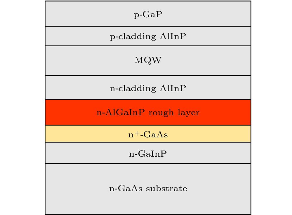
    Fig. 1. Schematic diagrams of AlGaInP-base LED epitaxial structure.
    Schematic diagrams of (a) conventional n-side-up AlGaInP LED structure and (b) n-AlGaInP contact LED.
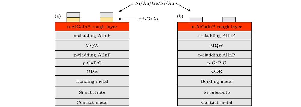
    Fig. 2. Schematic diagrams of (a) conventional n-side-up AlGaInP LED structure and (b) n-AlGaInP contact LED.
    I-V behaviors of Sample D5, ring intervals are 10−35 µm
    Fig. 3. I-V behaviors of Sample D5, ring intervals are 10−35 µm
    I-V behaviors of Sample A1, B1, C1 and D1 after annealing at 385 ℃ for 25 s.
    Fig. 4. I-V behaviors of Sample A1, B1, C1 and D1 after annealing at 385 ℃ for 25 s.
    Contact resistivity as a function of doping concentration for different annealing conditions.
    Fig. 5. Contact resistivity as a function of doping concentration for different annealing conditions.
    SIMS depth profiles of Ni/Au/Ge/Ni/Au contact on n-(Al0.27Ga0.73)0.5In0.5P before annealing and after annealing.
    Fig. 6. SIMS depth profiles of Ni/Au/Ge/Ni/Au contact on n-(Al0.27Ga0.73)0.5In0.5P before annealing and after annealing.
    At the same ND (a) ρc as a function of annealing temperature when the annealing time is 25 s; (b) ρc as a function of annealing temperature when the annealing temperature is 445 ℃.
    Fig. 7. At the same ND (a) ρc as a function of annealing temperature when the annealing time is 25 s; (b) ρc as a function of annealing temperature when the annealing temperature is 445 ℃.
    SEM micrographs showing the surface morphologies of ohmic contact (a) 445 ℃ for 25 s (b) 485 ℃ for 25 s.
    Fig. 8. SEM micrographs showing the surface morphologies of ohmic contact (a) 445 ℃ for 25 s (b) 485 ℃ for 25 s.
    编号ND/cm-3T/℃ Time/sρc/Ω·cm2编号ND/cm-3T/℃ Time/sρc/Ω·cm2
    A17 × 101738525C12 × 1018385251.1 × 10–3
    A27 × 101742525C22 × 1018425259.4 × 10–4
    A37 × 101744525C32 × 1018445254.8 × 10–4
    A47 × 1017485252.9 × 10–3C42 × 1018485255.3 × 10–4
    A57 × 10174456003.2 × 10–3C52 × 10184456002.8 × 10–4
    A67 × 10174459003.6 × 10–3C62 × 10184459003.0 × 10–4
    B11 × 101838525D13 × 1018385254.9 × 10–4
    B21 × 101842525D23 × 1018425254.0 × 10–4
    B31 × 1018445253.5 × 10–3D33 × 1018445253.3 × 10–4
    B41 × 1018485255.1 × 10–4D43 × 1018485254.1 × 10–4
    B51 × 10184456004.6 × 10–4D53 × 10184456001.4 × 10–4
    B61 × 10184459005.4 × 10–4D63 × 10184459001.9 × 10–4
    Table 1. Grouping information of samples annealing and specific contact resistivity (ρc) results.
    Su-Jie Wang, Shu-Qiang Li, Xiao-Ming Wu, Fang Chen, Feng-Yi Jiang. Study on the effect of thermal annealing process on ohmic contact performance of AuGeNi/n-AlGaInP[J]. Acta Physica Sinica, 2020, 69(4): 048103-1
    Download Citation