• Journal of Inorganic Materials
  • Vol. 36, Issue 1, 95 (2021)
Lu SHEN1, Dewen WANG2, Rong HUANG3, Shiyu DU1, and Qing HUANG1、*
Author Affiliations
  • 1Ningbo Institute of Materials Technology and Engineering, Chinese Academy of Sciences, Ningbo 315201, China
  • 2Shanghai Institute of Ceramics, Chinese Academy of Sciences, Shanghai 200050, China
  • 3Key Laboratory of Polar Materials and Devices (MOE), Department of Electronics, East China Normal University, Shanghai 200062, China
  • show less
    DOI: 10.15541/jim20190564 Cite this Article
    Lu SHEN, Dewen WANG, Rong HUANG, Shiyu DU, Qing HUANG. Electron Irradiation Induced Phase-separation Behavior in AlF3 Doped Alumina Ceramic with Superior Sensitivity[J]. Journal of Inorganic Materials, 2021, 36(1): 95 Copy Citation Text show less

    Abstract

    An electron irradiation induced fast phase-separation behavior was observed under convention Transmission electron microscopy (TEM) observation of spark plasma sintered AlF3 doped alumina ceramic. Spherical nanocrystalline Al precipitates separated out from original alumina grain surface within several seconds under transmission electron microscopy electron irradiation. By high resolution TEM observation combined with diffraction patterns analysis, it was found that the original alumina grain surface was in highly defected state. After electron irradiation under TEM, the defects on original alumina surface vanished accompanied by the precipitation of nanocrystalline Al particles. By thoroughly analysis of the defect reaction during doping process and the feature of cation sub-lattice of alumina, a defect assisted interstitial atom segregation mechanism was proposed to explain this behavior. According to this mechanism, doped F ions first occupied oxygen vacancy sites with corresponding Al ions at intrinsic interstitial sites. After oxygen vacancies being fully occupied, both F and Al ions tended to settle down at intrinsic octahedron interstitial sites, which resulted in a metastable doping state. Under the act of 1/3 [11ˉ00] partial dislocation of alumina matrix, distorted cation sub-lattice generated double aggregated vacant octahedron sites. When these doublets vacant octahedron sites were occupied by foreign Al ions, stacking faults composed of about three sequences were generated as that observed in high resolution TEM. Meanwhile, the segregated doping Al ions at double aggregated octahedron sites along the stacking faults worked as early stage precipitations. Under electron irradiation, with the ablation of F ions, the unstable segregated Al ions separated out as nano precipitation with the reconstruction of alumina lattice.

    Materials with good irradiation damage tolerance are necessary for modern unclear equipment as core components while those with good irradiation sensitivity can be applied as sensors and detectors for irradiation environment. The study of irradiation effect under various conditions is a prerequisite to screen suitable candidates for both applications. As for the electron irradiation, besides the typical linac irradiation devices, TEM is an alternatively simple and effective method in studying electron irradiation effect, especially for in-situ study[1,2,3,4,5,6,7,8,9,10,11,12,13,14,15].

    Alumina is one of the most extensively used structural ceramics and its electron irradiation effects have been well studied. Under conventional TEM observation (accelerate voltage no more than 300 kV, room temperature, and ordinary vacuum of ~10-5 Pa) a relative stable nature of alumina was found and only lattice defects like surface faceting[2], stacking fault[3,4] or localized structure degradation[5] were created. When the irradiation condition became critical, decomposition of Al2O3 and Al precipitation could be found. Conditions reported for Al precipitating from alumina matrix under TEM observation were relative extreme like high accelerate voltage (above 400 kV)[6,7], high temperature (above 700 K)[6,7,8,9], ultra-high dose rate[10,11] or ultra-high vacuum[2]. Bonevich, et al[2] reported that metallic Al formed on the surface after 1 h irradiation under ultra-high vacuum (10-8 Pa) while only surface faceting took place under conventional TEM exposure (vacuum of 10-5 Pa). Bouchet, et al[10] confirmed the reduction of alumina under extremely high dose rate through analyzing the energy loss near edge structure from the EELS results (Electron Energy Loss Spectroscopy, EELS), however, no metallic Al crystals could be directly observed. Until now, the easiest condition for Al fast precipitating from pure alumina under TEM observation was reported by Chen, et al[8,9] at temperature above the melting point of Al.

    Recently, we reported that transparent alumina ceramic could be easily sintered by SPS with AlF3 doping[12]. The present study is to reveal the microstructure character of the AlF3 doped Al2O3 by conventional TEM. Interestingly, a novel electron irradiation induced fast phase-separation behavior was observed. Aluminum nano-crystals separated out quickly from original highly defected Al2O3 grains, and the grain resulted in well crystallized state after conventional HRTEM observation.

    1 Experimental

    The 0.1wt% AlF3 doped alumina ceramic was sintered by SPS with parameters same to our previous report[12]. To obtain a separated grain for TEM observation, ceramic fragments were firstly scratched from the surface of sintered body with a diamond pen. Then the scratched fragments were treated by ultrasonic in ethanol to break the connected boundaries. Finally, the obtained grain suspension was dropt on copper grid for TEM observation. The observation was conducted with two transmission electron microscopes (TEM, JEM2100 and JEM2000F, JEOL, Japan).

    2 Results and discussion

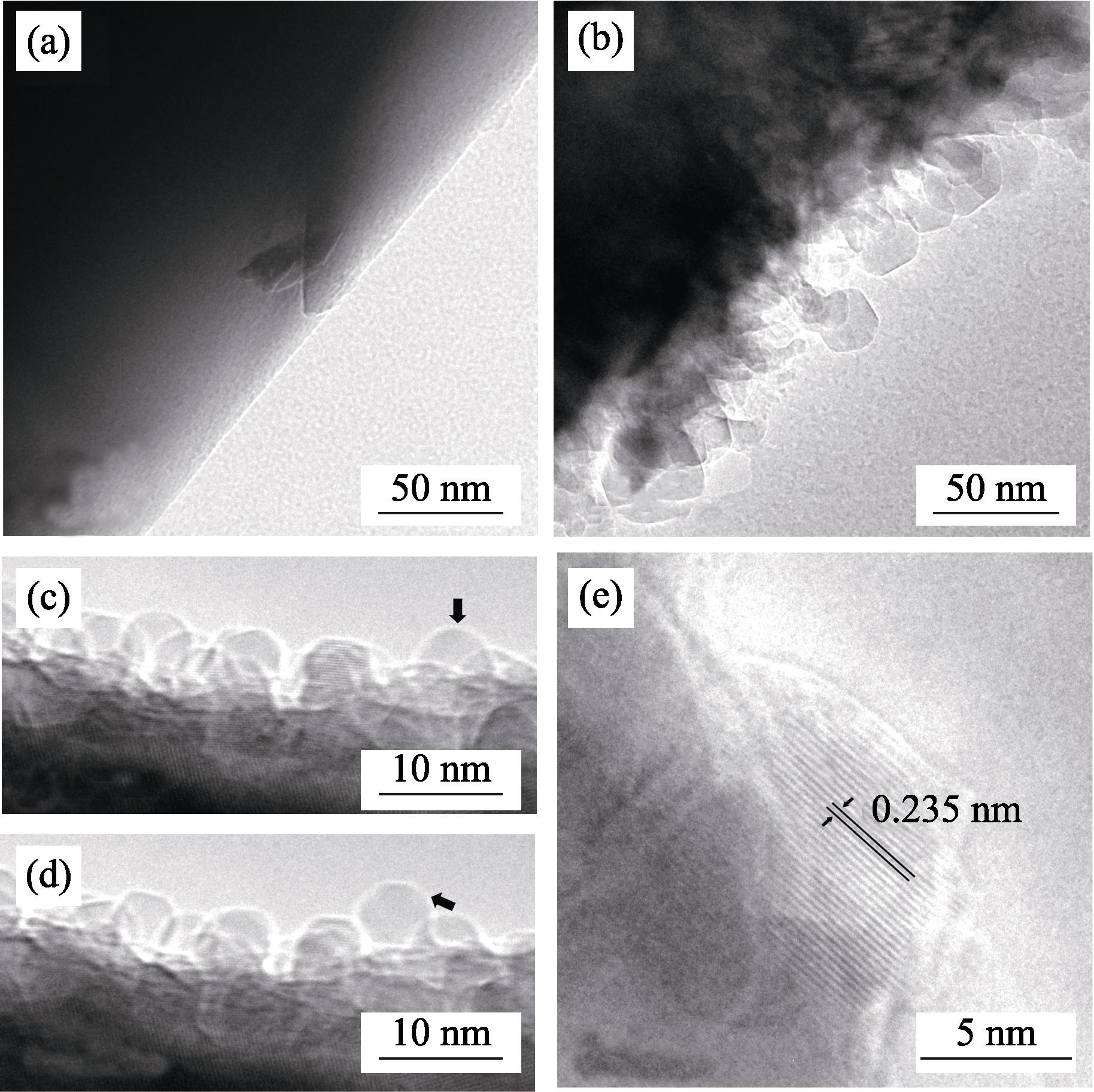
    Fig. 1(a) is a clean grain surface stripped from surrounding grains by ultrasonic break. The surface was stable under low magnification observation and no attached second phase was observed. However, once the magnification exceeded 200 k magnification, the surface became unstable. Moveable and growing precipitates were emitted from the surface under electron irradiation after several to dozens of seconds. The precipitates were sphere-like separated out at the beginning and generally transformed to faceted shape when lowering magnification or moving observation area. The diameter of these precipitates ranged from 5 to 50 nm. The typical feature of these precipitations displayed in Fig. 1(b). Arrows in Fig. 1(c-d) exhibited the growing of a precipitate accompanied with the decrease of another. The whole process finished within less than 5 s. Moreover, as a general case, when two growing precipitates contacted with each other, instantaneously they coalesced into a whole. The drop-like moving and coalescing behavior indicates a doubtable liquid-like nature of these precipitates. After the spherical-to-faceted transition, lattice fringes were easy to be seen. The 0.235 nm fringe space of the precipitation corresponds to the 0.234 nm-spacing (111) plane of metallic Al (Fig. 1(e)). The precipitates from original alumina matrix were further confirmed to be metallic Al by EELS study of the Al-L23 edges of the precipitation layers. In Fig. 2, Each feature peaks are identical with the reference spectrum of Al metal.

    TEM observations of a grain surface of 0.1wt% AlF3 doped sample (a) Original surface before high magnification observation; (b) Surface after high magnification observation, where sphere precipitates separated out; (c-d) Black arrow shows the growing of a new precipitate under irradiation; (e) Lattice fringes of a precipitated crystal

    Figure 1.TEM observations of a grain surface of 0.1wt% AlF3 doped sample (a) Original surface before high magnification observation; (b) Surface after high magnification observation, where sphere precipitates separated out; (c-d) Black arrow shows the growing of a new precipitate under irradiation; (e) Lattice fringes of a precipitated crystal

    Though it was reported that α-alumina is relatively stable under conventional TEM electron irradiation, the decomposition to Al under electron irradiation is a feature of AlF3 as described in previous studies[13,14,15]. In Ghatak, et al’s experiment, AlF3 was not stable under electron exposure and separated into localized 50 nm spherical Al crystals with fast fluorine ablation[15]. The resulted Al crystals are quite similar to the present observed precipitates, thus it is reasonable to conclude that the Al separation under electron irradiation is not the intrinsic property of alumina matrix but an extrinsic feature come from AlF3 doping. First, the conventional TEM observation only results in lattice defeats in alumina[2,3,4,5]. Bonevich, et al[2] reported that the original smooth surface became highly faceted under conventional 100 or 300 kV TEM electron irradiation with prolonged observation time. Tomokiyo, et al[3] found that planar defects and holes with preferred orientation could be produced near the surfaces under 200 kV TEM observation. Recently, Chen, et al[5] found that under HRTEM observation (vacuum lower than 10-6 Pa), phase transformation of thermal stable α-alumina to metastable κ’ phase occurred under 100 kV electron irradiation. Unfortunately, no Al precipitation was observed in all these studies. Moreover, different from the electron-irradiation- induced lattice defects in alumina[2,3], the present precipitation of Al crystalline resulted in a defect-free state from the original one carried stacking faults, as will be discussed in the following paragraphs. Second, the typical precipitation of Al under critical TEM condition accompanies with holing alumina matrix due to mass transportation[3-4,7-9,11], while it is not the present case since no apparent holing is observed and the surface becomes stable again once after precipitation of Al crystals.

    EELS of the precipitation and its reference

    Figure 2.EELS of the precipitation and its reference

    It will be easy to understand this behavior if the AlF3 was preferentially segregated at the surface. To further understand the phase-separation behavior and make clear the character inside a grain, another HRTEM and selected area diffraction were conducted with JEM-2100F. However, the results shown in Fig. 3(a-d) don’t seem to favor this assumption. Fig. 3(a) shows an original grain before irradiation induced Al precipitation. The white arrows point to the dark liner contrasts which suggesting the existence of planer defects. Diffraction pattern of the original grain is shown in Fig. 3(c), where the bright streaks identical with the liner contrasts in Fig. 3(a) confirm the existence of planer defects through the whole grain. It is interesting to note that, once after the Al precipitation by electron irradiation (Fig. 3(b)), the streaks in diffraction pattern of the same grain disappeared (Fig. 3(c)), indicating the precipitation of Al involved the reconstruction of lattice and finally resulted in a defect free state. Fig. 3(e) is the magnification of area i in Fig. 3(a), where the white dotted box traces a burgers circuit of an edge dislocation and the white arrow points the Burgers vector. An extra half atom plane can be clearly seen in the center of the box. Fig. 3(f) is the inversed FFT of area (ii) in Fig. 3(a) from (21¯1¯0)/(2¯110) diffraction spots, where many extra half-planes with dislocation mark can be seen, indicating the highly defected nature.

    HRTEM images and selected area diffraction of AlF3 doped alumina grain (a) HRTEM images of AlF3 doped alumina grain before Al precipitation. White arrows points to the planer defects; (b) The same grain after Al precipitation; (c, d) Diffraction patterns correspond to the grain before and after Al precipitation, respectively. The zone axis is along [0001] direction; (e) Magnification of area i in (a). The dotted box traces a dislocation core and the parallel lines show the distortion contrast composed of three or four layers; (f) Inversed FFT of the area ii in (a) from (21¯1¯0)/(2¯110) diffraction spots

    Figure 3.HRTEM images and selected area diffraction of AlF3 doped alumina grain (a) HRTEM images of AlF3 doped alumina grain before Al precipitation. White arrows points to the planer defects; (b) The same grain after Al precipitation; (c, d) Diffraction patterns correspond to the grain before and after Al precipitation, respectively. The zone axis is along [0001] direction; (e) Magnification of area i in (a). The dotted box traces a dislocation core and the parallel lines show the distortion contrast composed of three or four layers; (f) Inversed FFT of the area ii in (a) from (21¯1¯0)/(2¯110) diffraction spots

    Two kinds of defects reactions often involve in the doping process, namely substitution-vacancy and interstitial processes. The reaction equation can be written as below in the present case:

    $\text{Al}{{\text{F}}_{\text{3}}}\xrightarrow{\text{A}{{\text{l}}_{\text{2}}}{{\text{O}}_{\text{3}}}}\text{A}{{\text{l}}_{\text{Al}}}+\text{3F}_{\text{O}}^{\bullet }+{{\text{{V}'''}}_{\text{Al}}}$
    $\text{Al}{{\text{F}}_{\text{3}}}\xrightarrow{\text{A}{{\text{l}}_{\text{2}}}{{\text{O}}_{\text{3}}}}\text{3}{{{l}'}_{\text{F}}}+l_{\text{Al}}^{\centerdot \centerdot \centerdot }$

    Since the Al precipitated without holing the obvious matrix, it is hard to image the vacancy type reaction (1) dominates since the precipitated Al would be otherwise easier to settle down at Al vacancies. On the other hand, oxide ceramics sintered by SPS often accompanies oxygen vacancies due to the graphite surroundings and chamber vacuum[16,17]. Wang, et al[16] reported that excellent green emission caused by oxygen vacancies was observed in SP-sintered ZnO ceramic due to the vacuum ambience. The oxygen vacancies raised during SP-sintering process also resulted in degraded transparency in Y2O3 as reported by Jiang, et al[17]. Thus, it is reasonable to speculate that the doped F- ions first occupy oxygen vacancy sites with corresponding Al3+ at intrinsic interstitial sites. After oxygen vacancies being fully occupied, both F- and Al3+ tend to settle down at intrinsic interstitial sites as reaction (2). In this case, the settlement of extrinsic doping ions at oxygen vacancies or vacant interstitial sites will block the diffusion path of intrinsic Al3+ and O2- ions and inhibit the sintering process, which is quite identical to what we found recently by microstructure evolution analysis——AlF3 doping working as diffusion inhibitor during the sintering process. However, it is generally unstable for extra F- anions to settle down at octahedron vacancy sites due to the surrounding electrostatic repulsion. This means that the system may be in metastable state, which is perhaps the root cause of the phase- separation behavior. Moreover, the doping of F- was supposed to react with carbon contamination and emitted as gas products (CF)x in previous researches[18,19]. If this reaction exists within the sample, the solid dissolved F- and Al3+ ions may be non-stoichiometric with surplus Al3+ ions in alumina matrix.

    Considering that the bright streaks in diffraction pattern (Fig. 3(c)) and the corresponding liner contrasts in HRTEM (Fig. 3(a)) are quite similar to the feature of GP zones[20], the liner contrasts may be the segregations of Al atoms or ions in the form of early stage Al precipitates[3,4].

    Fig. 4(a) shows an ideal cation lattice diagram of alumina as suggested by Tomokiyo, et al[3]. Each circle represents an oxygen octahedron site. The oxygen sub-lattice is omitted to give a clearer illustration of the vacancies. The fluctuation of Al ions along C axis is also ignored. One third of the octahedron site remains unoccupied as shown by the open circles. The half-filled circles in (2¯110) plane illustrate the preferential occupation of foreign Al ions, which results in the segregation of Al ions and the corresponding mono-layer planer defects. More specifically, when combining the atomic character revealed in Fig. 3(e) and the real lattice structure, a clearer dislocation assisted mechanism can be proposed. In α-alumina, the {12¯10}<101¯0> prism plane slip is the secondary slip system beside the primary basal slip system and the <101¯0> prism plane dislocations are easy to dissociate to three 1/3 <101¯0> partial dislocations[21,22]. Fig. 4(b) is the real alumina structure under the projection of [112¯0] direction. The red dotted line includes two oxygen layers and a fluctuated Al layer inside the oxygen octahedrons. This selected Al layer is repainted under [0001] projection in Fig. 4(c). The open circles inside each Al hexagon represent unoccupied octahedron sites. Triangles at the right side indicate the normal stacking sequence A-B-A-B between two Al layers along [112¯0] direction. The red arrow at the left side represents a Burgers vector of 1/3 [11¯00] and dotted line in the center shows the slip or distorting plane. Whether after the passage of a movable 1/3 [11¯00] partial dislocation or distorted by the existence of a Frank partial dislocation with the same Burgers vector, the deformed atomic structure is shown in Fig. 4(d). The act of a 1/3 [11¯00] partial dislocation finally results in a stacking fault between the slip plane, and the distorted cation sub-lattice generates a double aggregated vacancy site (Fig. 4(d)). When these doublets vacancies are fully occupied by foreign Al ions, a stacking fault composed of three sequences is generated. This supposed condition is confirmed by the HRTEM in Fig. 3(e), where a distorted contrast composed of three to four layers beside a 1/3 [11¯00] partial dislocation can be found. As a result, the present defected grain nature can be regarded as planer defects assisted dissolving of AlF3 into alumina lattice, and in turn, interstitial Al3+ ions preferentially segregated at cation vacancies along the stacking faults as early stage precipitations. These segregations are unstable under electron irradiation especially after F- ablation, and finally separate out as precipitation with the reconstruction of cation lattice.

    (a) Schematic diagram of cation sub-lattice in α-alumina. The open and closed circles are the unoccupied and occupied octahedron sites respectively. Half-filled circles represent octahedron sites occupied by extrinsic Al3+ ions; (b) Real alumina structure in [112¯0] projection. The red box selects an Al layer between two oxygen layers; (c, d) Structures of the selected Al ions layer repainted in [0001] projection, before and after the act of a 1/3 [11¯00] partial dislocation, respectively. The open circles indicate unoccupied octahedron sites in the same layer

    Figure 4.(a) Schematic diagram of cation sub-lattice in α-alumina. The open and closed circles are the unoccupied and occupied octahedron sites respectively. Half-filled circles represent octahedron sites occupied by extrinsic Al3+ ions; (b) Real alumina structure in [112¯0] projection. The red box selects an Al layer between two oxygen layers; (c, d) Structures of the selected Al ions layer repainted in [0001] projection, before and after the act of a 1/3 [11¯00] partial dislocation, respectively. The open circles indicate unoccupied octahedron sites in the same layer

    It is also interesting to note that, LiF has a similar but more sensitive behavior under electron exposure like AlF3[15]. However, there is no such report so far (to our best knowledge) on the decomposition of LiF doped ceramics (especially for transparent spinels and garnets) under TEM observation even it is quite common for a doping concentration higher than 1%[18-19,23]. This may be due to the intrinsic differences of the defects structure or doping mechanism. Further characterization of LiF doped alumina or AlF3 doped spinel may be helpful to understand the role of fluoride sintering additives.

    3 Conclusions

    Until now, we found a novel fast electron-irradiation- induced phase-separation behavior in AlF3 doped alumina ceramic, which is never reported before. The original grain of the spark plasma sintered sample carried many planer defects with HRTEM observation, Al nano-crystal separated out with these planer defects disappearing. A defects assisted interstitial segregation mechanism was proposed to explain this behavior.

    References

    [1] K KANEKO, T KATO, M KITAYAMA et al. Precipitation of MgO. nAl2O3 in Mg-Doped α-Al2O3 under electron irradiation. Journal of the American Ceramic Society, 86, 161-168(2003).

    [2] E BONEVICH J, D MARKS L. Electron radiation damage of α-alumina. Ultramicroscopy, 35, 161-166(1991).

    [3] Y TOMOKIYO, T MANABE, C KINOSHITA. Structural change induced near surfaces of α-Al2O3 during electron irradiation.. Microscopy Microanalysis Microstructures, 4, 331-339(1993).

    [4] Y TOMOKIYO, T KUROIWA, C KINOSHITA. Defects occurring at or near surfaces in α-Al2O3 during electron irradiation. Ultramicroscopy, 39, 213-221(1991).

    [5] L CHEN C, K ARAKAWA, G LEE J et al. Electron-irradiation- induced phase transformation in alumina. Scripta Materialia, 63, 1013-1016(2010).

    [6] H OH S, Y KAUFFMANN, C SCHEU et al. Ordered liquid aluminum at the interface with sapphire. Science, 310, 661-663(2005).

    [7] P PELLS AERE G, T SHIKAMA. Radiation damage in pure and helium-doped α-Al2O3 in the HVEM Quantitative aspects of void and aluminium precipitate formation. Philosophical Magazine A, 48, 779-794(1983).

    [8] L CHEN C, H FURUSHO, H MORI. In situ TEM observation of decomposition of high-purity sapphire. Philosophical Magazine Letters, 89, 113-119(2009).

    [9] L CHEN C, H FURUSHO, H MORI. Effects of temperature and electron energy on the electron-irradiation-induced decomposition of sapphire. Philosophical Magazine Letters, 90, 715-721(2010).

    [10] D BOUCHET, C COLLIEX. Experimental study of ELNES at grain boundaries in alumina: intergranular radiation damage effects on Al-L23 and OK edges. Ultramicroscopy, 96, 139-152(2003).

    [11] D BERGER S, G SALISBURY I, H MILNE R et al. Electron energy-loss spectroscopy studies of nanometre-scale structures in alumina produced by intense electron-beam irradiation. Philosophical Magazine B, 55, 341-358(1987).

    [12] D WANG, L SHEN, S RAN et al. Transparent alumina fabricated by SPS sintering with AlF3 doping. Scripta Materialia, 92, 31-34(2014).

    [13] S CHEN G, B BOOTHROYD C, J HUMPHREYS C. Electron- beam induced crystallization transition in self-developing amorphous AlF3 resists. Applied Physics Letters, 69, 170-172(1996).

    [14] C MA, Y BERTA, L WANG Z. Patterned aluminum nanowires produced by electron beam at the surfaces of AlF3 single crystals. Solid State Communications, 129, 681-685(2004).

    [15] J GHATAK, T GNANAVEL, W GUAN et al. Electron Beam Synthesis of 3D Metal Nanostructures from Fluoride Precursors. MRS Online Proceedings Library Archive, 1411(2012).

    [16] J WANG, L GAO. Photoluminescence properties of nanocrystalline ZnO ceramics prepared by pressureless sintering and spark plasma sintering. Journal of the American Ceramic Society, 88, 1637-1639(2005).

    [17] T JIANG D, K MUKHERJEE A. The influence of oxygen vacancy on the optical transmission of an yttria-magnesia nanocomposite. Scripta Materialia, 64, 1095-1097(2011).

    [18] S MEIR, S KALABUKHOV, N FROUMIN et al. Synthesis and densification of transparent magnesium aluminate spinel by SPS processing. Journal of the American Ceramic Society, 92, 358-364(2009).

    [19] I REIMANIS, J KLEEBE H. A review on the sintering and microstructure development of transparent spinel (MgAl2O4). Journal of the American Ceramic Society, 92, 1472-1480(2009).

    [20] B WILLIAMS D, B CARTER C. Transmission Electron Microscopy: a Textbook for Materials Science, 2nd edition, 271-282(2009).

    [21] H HEUER A, D LAGERLOF K P, J CASTAING. Slip and twinning dislocations in sapphire (α-Al2O3). Philosophical Magazine A, 78, 747-763(1998).

    [22] M CASTILLO-RODRIGUEZ, A MUNOZ, J CASTAING et al. Basal slip latent hardening by prism plane slip dislocations in sapphire(α-Al2O3). Acta Materialia, 58, 5610-5619(2010).

    [23] R MARDER, R CHAIM, G CHEVALLIER et al. Effect of 1wt% LiF additive on the densification of nanocrystalline Y2O3 ceramics by spark plasma sintering. Journal of the European Ceramic Society, 31, 1057-1066(2011).

    Lu SHEN, Dewen WANG, Rong HUANG, Shiyu DU, Qing HUANG. Electron Irradiation Induced Phase-separation Behavior in AlF3 Doped Alumina Ceramic with Superior Sensitivity[J]. Journal of Inorganic Materials, 2021, 36(1): 95
    Download Citation