Tieshan Yang, Han Lin, Baohua Jia, "Ultrafast direct laser writing of 2D materials for multifunctional photonics devices [Invited]," Chin. Opt. Lett. 18, 023601 (2020)
Search by keywords or author
- Chinese Optics Letters
- Vol. 18, Issue 2, 023601 (2020)
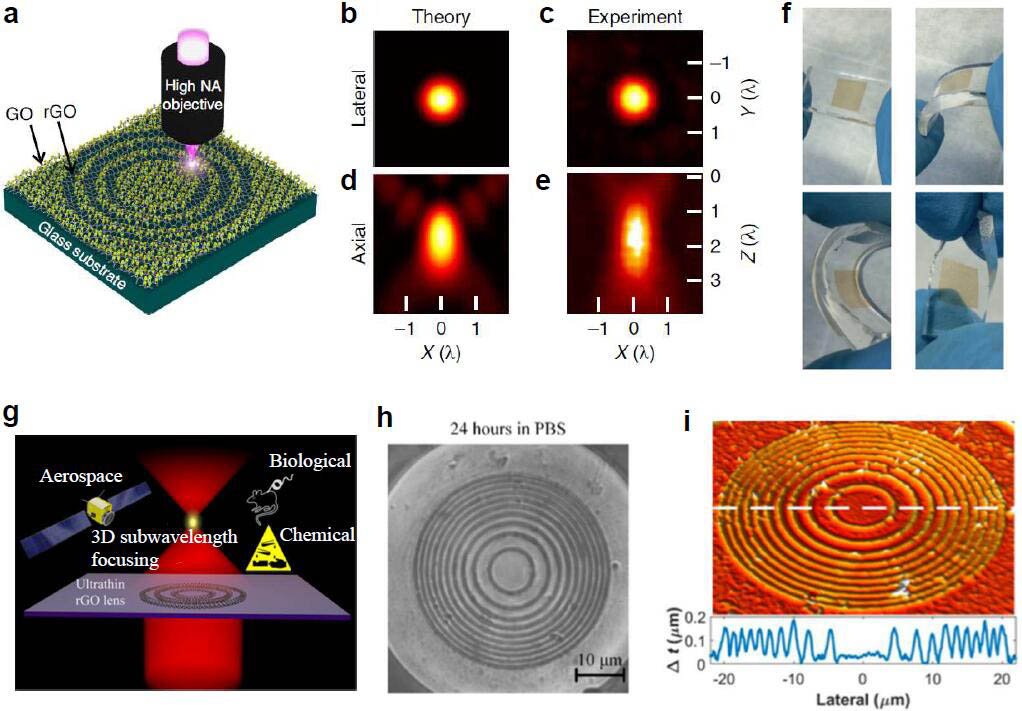
![(a) Conceptual design and laser fabrication of the GO ultrathin lens. (b), (d) Theoretical focal intensity distributions in the lateral and axial directions. (c), (e) Experimental focal intensity distributions along the lateral and axial directions. (f) Bending and twisting of the GO thin film on a polydimethylsiloxane substrate. (a)–(f) Reproduced with permission[43]. Copyright 2015, Nature Publishing Group. (g) Graphene ultrathin flat lens working in harsh environment. rGO lens after the PBS test. (h) Microscopic image of the rGO lens after immersing in PBS for 24 h. (i) Topological profile of the rGO lens after PBS test. (g)–(i) Reproduced with permission[57]. Copyright 2018, American Chemical Society.](/richHtml/col/2020/18/2/023601/img_001.jpg)
Fig. 1. (a) Conceptual design and laser fabrication of the GO ultrathin lens. (b), (d) Theoretical focal intensity distributions in the lateral and axial directions. (c), (e) Experimental focal intensity distributions along the lateral and axial directions. (f) Bending and twisting of the GO thin film on a polydimethylsiloxane substrate. (a)–(f) Reproduced with permission[43]. Copyright 2015, Nature Publishing Group. (g) Graphene ultrathin flat lens working in harsh environment. rGO lens after the PBS test. (h) Microscopic image of the rGO lens after immersing in PBS for 24 h. (i) Topological profile of the rGO lens after PBS test. (g)–(i) Reproduced with permission[57]. Copyright 2018, American Chemical Society.
![(a) Optical image of a fabricated monolayered WS2 lens. (b) Theoretical focal intensity distributions in the lateral directions. (c) Experimental focal intensity distributions along the lateral directions. (d) Intensity distribution of the theoretical and experimental results along the lateral directions. Reproduced with permission[44]. Copyright 2016, Conference on Lasers and Electro-Optics (CLEO).](/richHtml/col/2020/18/2/023601/img_002.jpg)
Fig. 2. (a) Optical image of a fabricated monolayered
Fig. 3. (a)–(c) Schematic of the dynamic process for in situ phototunable graphene metamaterials. (d) SEM image of the five-layer GO structure clearly showing the layer-by-layer structure. (e) Optical micrographs of reduction and ablation of graphene metamaterials. Changes in (f) refractive index and (g) extinction coefficient as functions of laser power for graphene metamaterials at broadband wavelengths ranging from 200 to 1600 nm. Reproduced with permission[45]. Copyright 2019, American Chemical Society.
Fig. 4. (a) Schematic of graphene-based metamaterial absorber. (b) Photograph of the absorber with an area of 50 mm by 25 mm. (c) Optical microscope image of the grating. (d) SEM image of the central part of the grating. (e) Schematic of the set-up to measure the heating of the sample under sunlight. (f) Thermal image of the fabricated large-area absorber sample. (g) Temperature measurement of the GO metamaterial (red), the graphene-based metamaterial absorber (black), and hierarchical graphene foam (green). Reproduced with permission[46]. Copyright 2019, Nature Publishing Group.
Fig. 5. (a)–(c) rGO holograms by a single femtosecond pulse for 3D images with wide viewing angles and color images. (d)–(h) Vectorial holographic reconstruction of polarization discernible images. Reproduced with permission[60]. Copyright 2015, Nature Publishing Group.
Fig. 6. (a) Commission Internationale de L’Eclairage (CIE) coordinates corresponding to emissions of the thick NP and the laser-fabricated holes. Fluorescence micrographs of (b) thin nanoplatelets and (c) thick nanoplatelets without patterns. A 405 nm laser is used as excitation. (d) Microscopic image of nanoplatelets with laser patterned characters. (e) Fluorescence micrograph of the patterned nanoplatelets under laser excitation. Reproduced with permission[65]. Copyright 2019, American Chemical Society.

Set citation alerts for the article
Please enter your email address


