
Lu Liu, Yupeng Wang, Yunxiu Ma, Guogang Li, Zhigao Dai. Advances in In-Plane Hyperbolic Phonon Polaritons in Natural Layered Metamaterials[J]. Chinese Journal of Lasers, 2023, 50(1): 0113011
- Chinese Journal of Lasers
- Vol. 50, Issue 1, 0113011 (2023)
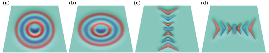
Fig. 1. Field distribution in z direction for different dielectrics. (a) In-plane isotropic dielectric (ɛx=ɛy>0); (b) in-plane elliptic dielectric (ɛx>0, ɛy>0, ɛx≠ɛy); (c) in-plane hyperbolic dielectric (ɛx<0, ɛy>0); (d) in-plane hyperbolic dielectric (ɛx>0, ɛy<0)
![Natural hyperbolic metamaterials. (a) Infrared hyperbolic hypersurface of hBN nanostructure[24]; (b) scanning electron microscope (SEM) image of hBN infrared hyperbolic hypersurface (nominal grating parameters are w≈75 nm and g≈25 nm); (c) tip launching phonon polaritons on hyperbolic hypersurface (indicated by simulated near fields); (d) schematic of unit cell of α-MoO3 with lattice constants a=0.396 nm, b=1.385 nm and c=0.369 nm; (e) in-plane elliptical and hyperbolic phonon polaritons in α-MoO3 disk; (f) thickness tunability of in-plane hyperbolic and elliptic phonon polaritons in α-MoO3[15]](/richHtml/zgjg/2023/50/1/0113011/img_02.jpg)
Fig. 2. Natural hyperbolic metamaterials. (a) Infrared hyperbolic hypersurface of hBN nanostructure[24]; (b) scanning electron microscope (SEM) image of hBN infrared hyperbolic hypersurface (nominal grating parameters are w≈75 nm and g≈25 nm); (c) tip launching phonon polaritons on hyperbolic hypersurface (indicated by simulated near fields); (d) schematic of unit cell of α-MoO3 with lattice constants a=0.396 nm, b=1.385 nm and c=0.369 nm; (e) in-plane elliptical and hyperbolic phonon polaritons in α-MoO3 disk; (f) thickness tunability of in-plane hyperbolic and elliptic phonon polaritons in α-MoO3[15]
Fig. 3. Controllable launching and focusing of hyperbolic phonon polariton. (a) Real-space imaging of edge-tailoring phonon polaritons at angle-dependent α-MoO3; (b) angle-dependent ke isofrequency contour of phonon polaritons in α-MoO3 at ω=889.8 cm-1; (c) edge modulated phonon polariton real-space image of isosceles triangles with different adjacent angles, squares and rectangles α-MoO3 nano-cavity with different rotation angles[23]; (d), (e) experimental near-field amplitude images in α-MoO3 microstructures of varied shapes of square, regular pentagon and regular hexagon microstructures at frequencies of 915 cm-1 and 986 cm-1[25]
Fig. 4. High efficiency launching and focusing of phonon polariton. (a) Real-space imaging of hyperbolic phonon polaritons on surface of natural 220-nm-thick α-MoO3 flake[27]; (b) near-field images of hyperbolic phonon polaritons launched by an Au disk nanoantenna fabricated on top of a 165-nm-thick α-MoO3 crystal[28]; (c) radius-of-curvature-dependent hyperbolic phonon polaritons in-plane focusing[29]
Fig. 5. Tunability of hyperbolic phonon polaritons. (a) Schematic showing nano-imaging of suspended α-MoO3 flake using scattering-type scanning near-field optical microscope (s-SNOM); (b), (c) images taken at frequencies of 937 cm-1 and 990 cm-1[32]. (d) Optical micrographs and s-SNOM amplitude images (890 cm-1) of MoO3 flake on SiO2/Si substrate before hydrogenation, 10 s after hydrogenation, and after dehydrogenation[33]
Fig. 6. Optical topological transformation of hyperbolic phonon polaritons. (a)-(l) Experimental observation of topological polaritons launched by air, twisted angles are Δθ=-44°, Δθ=65°, and Δθ=-77°, respectively[34]; (m)-(p) experimental observation of topological polaritons launched by air, twisted angles are Δθ=0°, Δθ=30°, Δθ=75°, and Δθ=90°, respectively[35]
Fig. 7. Topological transition of hybrid polaritons in graphene/α-MoO3 heterostructure. (a)-(l) Experimentally measured polariton near-field distributions with graphene doping Fermi energy of 0, 0.3, 0.7 eV[42]; (m)-(p) thickness dependent hybrid polaritons in graphene/α-MoO3 heterostructures with experimentally measured field distributions at 888 cm-1 and 900 cm-1[40]

Set citation alerts for the article
Please enter your email address
© Copyright 2018-2021 | Chinese Laser Press. All Rights Reserved 沪ICP备15018463号-20