
Jiuyuan Geng, Jianhua Yang, Ting Shu, Xinbing Cheng, Rong Chen. 10 GW dual-spiral Blumlein pulse forming lines in glycerol medium[J]. High Power Laser and Particle Beams, 2023, 35(6): 065004
- High Power Laser and Particle Beams
- Vol. 35, Issue 6, 065004 (2023)
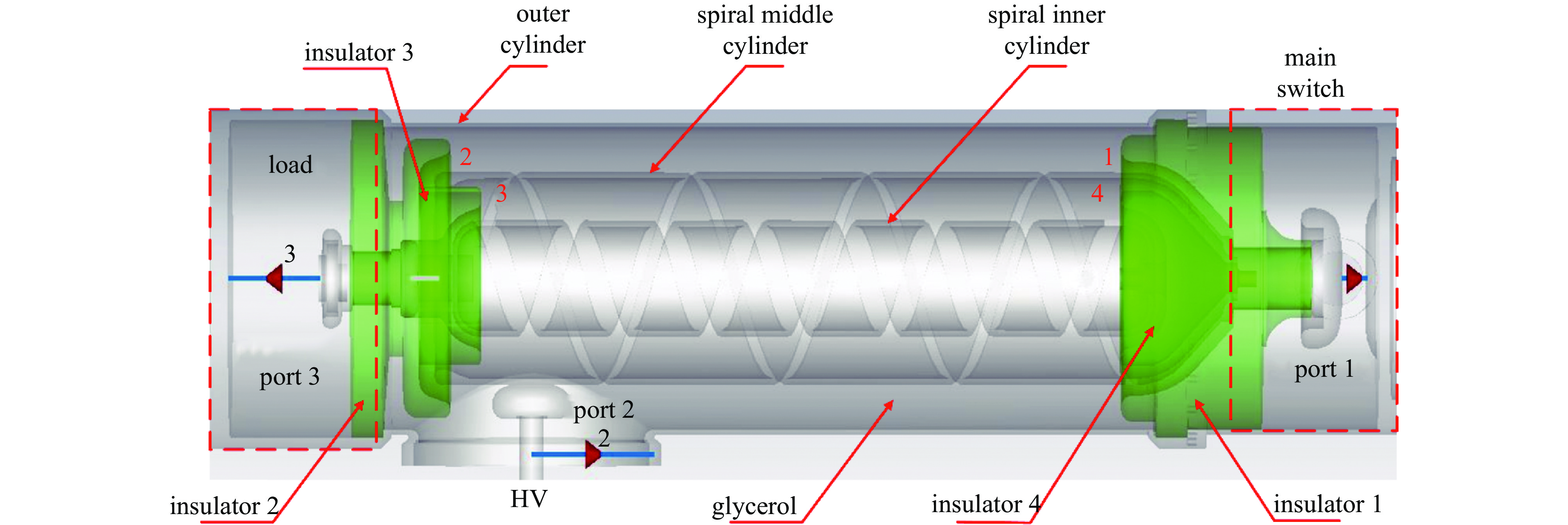
Fig. 1. Structure of dual-spiral BPFL
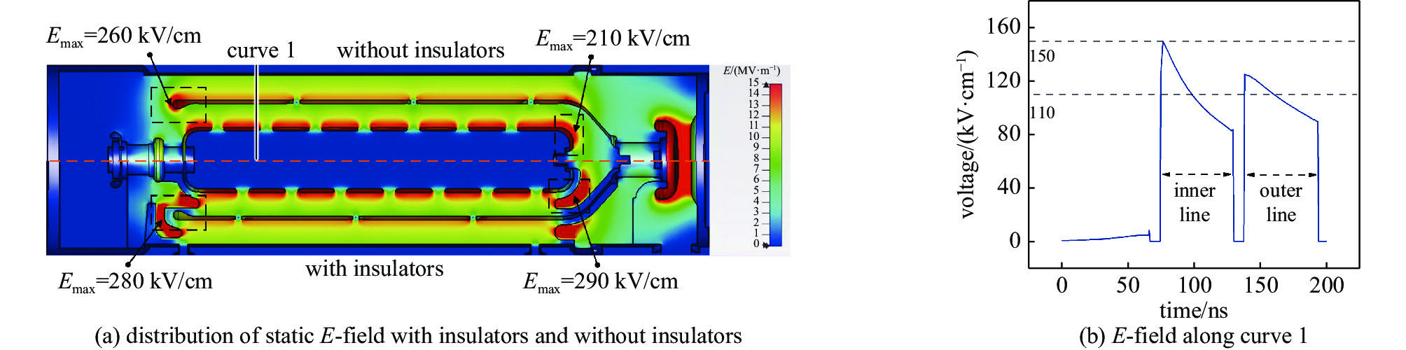
Fig. 2. Distribution of static E -field
Fig. 3. Schematic of EM/circuit co-simulation
Fig. 4. Typical output pulse of dual-spiral BPFL
Fig. 5. Transient E -field distribution of dual-spiral BPFL at different points in Fig.4
Fig. 6. Schematic diagram of traveling wave transmission in spiral BPFL during charging
Fig. 7. Effect ofN m on the output pulse (N i=7, L =120 nH)
Fig. 8. Effect of N i on the output pulse (N m=3, L =120 nH)
Fig. 9. Transient E-field distribution of dual-spiral BPFL during the rising edge (N i=1)
Fig. 10. Effect of switching inductance on the output pulse (N m=3, N i=7)
Fig. 11. Structure diagram of experimental device
Fig. 12. Breakdown of insulator 1 and improved measure
Fig. 13. 100 successive experimental waveforms at PRF of 10 Hz (blue waveform is the output voltage, light blue is the charging voltage, and yellow is the trigger signal)
Fig. 14. Experimental waveform and simulated output pulse
|
Table 1. Output pulse characteristic parameters with different N m
|
Table 2. Output pulse characteristic parameters with different N i
|
Table 3. Output pulse characteristic parameters with different switch inductance L (N m=3, N i=7)

Set citation alerts for the article
Please enter your email address
© Copyright 2018-2021 | Chinese Laser Press. All Rights Reserved 沪ICP备15018463号-20