1Key Lab of All Optical Network and Advanced Telecommunication Network of EMC, Institute of Lightwave Technology, Beijing Jiaotong University, Beijing 100044, China
2College of Physics and Engineering, Qufu Normal University, Qufu 273165, China
Hongyao Chen, Tigang Ning, Jing Li, Li Pei, Jin Yuan, Xiaodong Wen. Study on a v-band signals and pulses generator with a tunable optical carrier to sideband ratio[J]. Chinese Optics Letters, 2017, 15(6): 060605
Copy Citation Text
This Letter demonstrates a filterless v-band signals and pulses generator scheme with a tunable optical carrier to sideband ratio (OCSR). Through complete theoretical analysis, the mathematical expression of the OCSR that contains the extinction ratio, phase modulation index, and bias angle is obtained. It is found that the OCSR has a wide tuning range, from 50 to . By careful adjustment, a 60 GHz millimeter-wave signal with the OCSR at 50.72 dB and the electrical spurious suppression ratio at 36.6 dB can be achieved. Moreover, the discussions of using optimum OCSR to generate a Nyquist pulse or triangular-shaped pulse are also presented in this Letter.
With the accelerated development of optical communications, optical links have been widely used for the transmission of high-speed and large-capacity signals because of the inherent low loss, low dispersion, and wide bandwidth of fibers, added to the possibility of using optical amplifiers to compensate for the loss[1,2]. For similar reasons, the optical links in wireless/mobile communications has attracted increasing attention[3–7]. For example, radio over fiber (RoF) technology, which can deliver millimeter-wave (mm-wave) signals over long distances, is being considered for the efficient delivery of multimedia to users with its outstanding advantages of wireless signal transmission, such as improved coverage, flexibility, transparency, and low cost of deployment[8].
The key of the technology is the generation of mm-wave signals in the optical domain. During the last few decades, extensive investigations of optical mm-wave generation systems have led to many electrical-signal-generation methods, such as the optical phase-locked loop[9], optical injection locking[10], and external modulation[11–14]. Among these methods, external modulation has been regarded as the most promising method for high-quality mm-wave generation due to its simple implementation and assembly, high-frequency tunability, and low phase noise.
External-modulation-based mm-wave generation schemes are usually built using a laser source, a local oscillator, one or more Mach–Zehnder modulators (MZMs), and by coupling with optical filters that can generate mm-wave signals with a variety of characteristics, such as optical single sideband (OSSB)[11–13], high-frequency multiplication factor[14], and tunable optical carrier to sideband ratio (OCSR)[15]. These characteristics have been proven to be very useful for removing fiber dispersion-induced power fading, reducing the system cost, and improving the receiver sensitivity of fiber links. Not only that, the external modulation structure can also be used to generate pulse trains in the optical domain, such as Nyquist[16], triangular-shaped[17,18], and rectangular-shaped pulses[19], which can be used for wavelength conversion, light storage, and signal processing.
Sign up for Chinese Optics Letters TOC. Get the latest issue of Chinese Optics Letters delivered right to you!Sign up now
Although mm-wave signals and pulse trains generation can be realized with similar structures, a photonic generator scheme, which can realize optical mm-wave signals and pulse trains generation simultaneously, is not easily implemented.
In this Letter, we show and discuss a simple filterless method to overcome the limitations mentioned above. In principle, the method is based on cascading a dual-wavelength laser and a dual-parallel MZM (DP-MZM), which can generate optical carrier and sidebands with tunable OCSR, and the OCSR can be widely and continuously tuned from about 50 to . By using the tunable OCSR, we will link the mm-wave signals and pulses generation and offer the possibility of integrating mm-wave signals, Nyquist, and triangular-shaped pulses generation into a photonic generator with satisfactory spectral purity and flexible pulse widths.
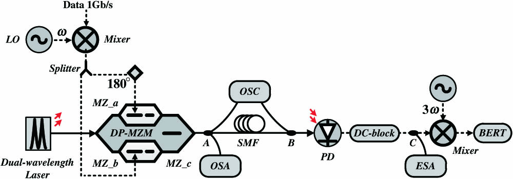
The proposed photonic generator scheme is shown in Fig. 1. The optical field at the input of the DP-MZM is generated by a dual-wavelength laser, which can be expressed as where denotes the amplitude of optical field, and and are the angular frequencies of the two optical carriers. Since the two wavelength components are generated simultaneously under the same structure, therefore, their phase is consistent, which is not shown in Eq. (1). The angular frequency interval is , so Eq. (1) can be further rewritten as
Figure 1.Block diagram of the proposed v-band signals and pulses generator scheme. LO, local oscillator; SMF, single mode fiber; OSA, optical spectrum analyzer; OSC, oscilloscope; PD, photodiode; ESA, electrical spectrum analyzer; BERT, bit error rate tester.
The electrical driving signal is generated by a local oscillator, which is divided into two paths to drive the two child Mach–Zehnder interferometers (MZIs), and in a parent MZIs, known as . The electrical driving signals sent to and are
When and operate at the minimum transmission point, the output field of the DP-MZM can be expressed as where represents the half-wave voltage, represents the bias voltage of , denotes the Bessel function of the first kind of order , is the phase modulation index, and is a weighting coefficient related to the extinction ratio () of the sub-MZMs.
When , the system is operating at weak modulation situation, where equals 0.039. The corresponding values of , , , and are 0.9996, 0.0196, , and , respectively. Thus, the optical sidebands higher than the first order can be neglected without significant error, and Eq. (6) can be simplified as where can also be simplified as When , the output field of the DP-MZM can be finally written as where equals So, the OCSR (in dB) of the generated optical signal can be calculated as where is a bias angle. From Eq. (11), we can conclude that the OCSR is a function determined by the phase modulation index , extinction ratio , and bias voltage . It means that by controlling these three parameters, we can achieve the OCSR with continuous adjustment characteristics.
OptiSystem 10.0 is chosen to perform the simulations and to verify the proposed scheme. The simulated setup is shown in Fig. 1. In our simulation, the frequency interval between two optical carriers is 20 GHz. It is the same with the electrical driving signal frequency. The linewidth of the dual-wavelength laser is 0.1 MHz, and the output power is 0 dBm. The phase modulation index of the DP-MZM is set as , and the extinction ratio is 20 dB. By adjusting the bias voltage of MZ_c, the continuous tunable characteristic of the OCSR can be found.
The calculation and simulation results are shown in Fig. 2. Figure 2(a) shows that with the increasing of bias voltage , the bias angle increases, and the OCSR changes continuously from about 50 to . The calculation line (black) is well fitted by the simulation dotted line (red), demonstrating that the mathematical derivation of the OCSR is valid. Moreover, the calculated OCSR performance as functions of bias angle under different extinction ratios is shown in Fig. 2(b). In Fig. 2(b), the tuning range of the OCSR is extended from about 50 to , and it indicates that the higher the extinction ratio is, the less sensitive the OCSR to bias angle would be, which means that we can increase the extinction ratio to improve the system stability.
Figure 2.Calculation and simulation results: (a) OCSR versus bias angle at calculation (black line) and simulation (red line) cases; (b) OCSR versus bias angle with a different extinction ratio (ER).
Here, consider that the carriers will be effectively suppressed when the OCSR is over 25 dB. Thus, Eqs. (9) and (10) can be simplified as
Two frequency components exist, which can be used to generate a mm-wave signal.
After being detected by a photodiode (PD), following the square-law detection with responsivity , the photocurrent of the generated frequency tripling signal can be expressed as
When equals 157.8°, the OCSR reaches the maximum value of 50.72 dB [point A in Fig. 2(a)], which meets the mm-wave signal generation condition. The optical spectrum at the output of the DP-MZM is shown in Fig. 3(a). Two strong optical sidebands with a frequency difference that is three times the frequency of the electrical driving signal exists, and the other optical sidebands are effectively suppressed. After PD detection, a 60 GHz frequency tripling v-band mm-wave signal can be generated. As seen in Fig. 3(b), a pure 60 GHz electrical signal can be obtained regardless of the single mode fiber (SMF) transmission. The electrical spurious suppression ratio (ESSR) exceeds 35.5 dB in the case of back-to-back (BTB) transmission, which is a little weaker than that in the 20 km SMF transmission (36.6 dB). It is because in the case of 20 km SMF transmission, double sideband modulation (DSB) signals will cause the power to periodically jitter, leading to the power reduction of the undesired harmonic electrical signals.
Figure 3.Simulation results of the proposed generator when equals 157.8°: (a) optical spectrum at the output of the DP-MZM; (b) electrical spectrum at the output of the PD without SMF transmission (red) and with 20 km SMF transmission(blue); (c) BER curves and corresponding eye diagram, BTB transmission (red), 20 km transmission (blue), and power penalty ().
In order to evaluate the transmission performance of the generated optical signal, data modulation is applied, which is generated by mixing a 1 Gbps pseudorandom bit sequence (PRBS) with the driving signal at a mixer. At the receiver, coherent demodulation is employed and a bit error rate tester (BERT) is used to catch the BER curves and corresponding eye diagram. The bit error rate (BER) curves and corresponding eye diagram are shown in Fig. 3(c). In the plot, two BER curves can both reach with a receiver sensitivity of less than 23.5 dB regardless of SMF transmission, and the corresponding eye diagram is widely open. The power penalty is less than 0.3 dB, which means that the generated mm-wave signal is satisfied.
In fact, since the DP-MZM is composed of two MZI structures, there are three bias voltages, , , and , to control the output spectrum. However, the bias voltage may drift when introduced by the temperature. Hence, we should think about it. With the help of simulation software, a detailed analysis of the voltage drift effect has been implemented. The simulation results are shown in Fig. 4. In Fig. 4(a), we only consider one of these three voltage drifts. Each of them will cause the OCSR attenuation, but and will play major roles (‘’, red line; ‘’, red dotted line; ‘’, blue line; ‘’, blue dotted line), which means that ensuring the bias voltage stability of the two sub-MZMs is more useful to the system. In Fig. 4(b), we consider the voltage drifts of and effects on the system. When the voltage drifts in the same direction (‘’, purple line purple; ‘’, purple dotted line), the OCSR performance is better than that of the opposite direction (‘’, orange line; ‘’, orange dotted line); therefore, we had better to keep the bias voltage drifts of the two sub-MZMs going in the same direction. Finally, we consider the superposition effect of three bias voltage drifts. The results of Figs. 4(a), 4(b), and 4(c) can confirm each other. In Fig. 4(c), the voltage drift direction of and stay identical, but also has satisfactory performance (‘’, black line; ‘’, black dotted line; ‘’, light gray line; ‘’, light gray dotted line). Moreover, through the corresponding eye diagram, we can see that the OCSR attenuation does not cause a great impact on the quality of transmission performance, the eyes are still widely open. It means that the variation caused by the voltage drift is also within the acceptable range.
Figure 4.Simulation and results of OCSR versus bias voltage drift: (a) the voltage drift effect of , , and , respectively; (b) the voltage drift superposition effect of and ; (c) the voltage drift superposition effect of , , and . (Note that for ease of expression, ‘’ represents voltage drift ranges from 0 to , ‘’ represents voltage drift ranges from to 0 mV, and ‘a, b, c’ represents the , , and , respectively. For example, ‘’ represents voltage drifts of the and , which ranges from 0 to , and the voltage drift of , which ranges from to 0 mV.)
In practice, a further discussion on OCSR is necessary, especially when the OCSR has a wide tuning range, so each particular OCSR will be very useful. When equals 102.6°, the OCSR is , which meets the optical generation condition of the triangular-shaped waveform [point B in Fig. 2(a)]. The optical spectrum at the output of the DP-MZM is shown in Fig. 5(a), where with proper dispersion, a triangular-shaped pulse train can be caught by an oscilloscope (OSC). Figure 5(b) shows the four pulse trains with different pulse durations, where the envelopes of four pulse trains are all triangular-shaped, and the pulse duration of the generated pulse train can be changed by adjusting the driving signal and the frequency interval of two optical carriers.
Figure 5.Simulation results of the proposed generator when equals 102.6°: (a) optical spectrum at the output of the DP-MZM; (b) the waveforms of the generated triangular-shaped pulses with different pulse durations (100 ps yellow line, 66.7 ps green line, 50 ps red line, 40 ps blue line).
By increasing to make equal to 180°, the OCSR reduces to 0 dB, which will satisfy the optical generation condition of the Nyquist waveform [point C in Fig. 2(a)]. The optical spectrum at the output of the DP-MZM is shown in Fig. 6(a). Four equispaced optical sidebands exist with 0.01 dB flatness, and the unwanted mode suppression ratio (UMSR) of the rectangular-shaped four-tones optical frequency comb (OFC) is more than 50 dB. Figure 6(b) shows the corresponding temporal Nyquist waveform with full width at half-maximum (FWHM) of 11.4 ps with the duty cycle of 22.8% (red line) and other three Nyquist pulse trains with different FWHMs and pulse durations.
Figure 6.Simulation results of the proposed generator when equals 180°: (a) optical spectrum at the output of the DP-MZM; (b) the waveforms of the generated Nyquist waveform pulses with different pulse durations (100 ps yellow line, 66.7 ps green line, 50 ps red line, 40 ps blue line).
In conclusion, a flexible and cost-effective v-band signals and pulses generator with tunable OCSR is proposed and theoretically demonstrated. We derive the mathematical expression and characteristic curve of the OCSR and discussed three particular points that can be used to generate mm-wave signals, Nyquist, and triangular-shaped pulses, respectively. With careful adjustment of the OCSR, a 60 GHz mm-wave signal with an OCSR of 50.72 dB, an ESSR of 36.6 dB, a triangular-shaped pulse train with flexible pulse widths, and a Nyquist pulse train with the duty cycle of 22.8% can be realized.
When compared with previous reported approaches, this work benefits from the advantage of a continuously tunable OCSR, which will offer the possibility of integrating mm-wave signals and pulses generation into a photonic generator. However, since a standard DP-MZM is required to realize the tunable OCSR, the bias voltage may drift if introduced by the temperature. A detailed discussion has been given in this Letter, and further study will be necessary to solve this problem.
Hongyao Chen, Tigang Ning, Jing Li, Li Pei, Jin Yuan, Xiaodong Wen. Study on a v-band signals and pulses generator with a tunable optical carrier to sideband ratio[J]. Chinese Optics Letters, 2017, 15(6): 060605