
Leiying Zhai, Liyu Zhao, Yijie Wang, Jingchang Nan. Research on Structured Light Projection Chips Based on Metasurfaces and MEMS[J]. Chinese Journal of Lasers, 2024, 51(6): 0613002
- Chinese Journal of Lasers
- Vol. 51, Issue 6, 0613002 (2024)
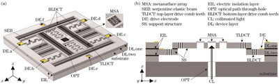
Fig. 1. Three-dimensional structural and cross-sectional diagrams of the structured light projection chip. (a) Three-dimensional structural diagram; (b) cross-sectional diagram
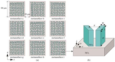
Fig. 2. Schematics of the metasurface array and nanopillar structure diagram. (a) Schematic of the metasurface array; (b) nanopillar structure diagram
Fig. 3. Hybrid coded structured light patterns
Fig. 4. Flowchart of GS algorithm
Fig. 5. Schematic of electrostatically driven comb structure
Fig. 6. Simulation of metasurface nanopillars. (a) Conversion efficiency of metasurface nanopillar dimensions to incident light versus incident wavelength; (b) relationship between rotation angle of metasurface nanopillars with normalized phase of incident light
Fig. 7. Phase of mixed coding structured light stripes
Fig. 8. Gray code and phase-shifted strips projected by metasurface units. (a) Gray code strips; (b) phase-shifted strips
Fig. 9. Light intensity distribution of Gray code strips. (a) Normalized optical intensity distribution along x-axis of Gray code strips; (b) envelope of the normalized optical intensity distribution
Fig. 10. Light intensity distribution of phase-shifted strips. (a) Normalized optical intensity distribution of phase-shifted strips; (b) fit curves of the normalized optical intensity distribution in the central region
Fig. 11. Relationship between displacement and drive voltage of 2D scanning platform
Fig. 12. Displacement and stress cloud maps. (a) Displacement cloud map of device layer 1; (b) stress cloud map of device layer 1; (c) displacement cloud map of device layer 2; (d) stress cloud map of device layer 2
Fig. 13. Modal results. (a) First mode; (b) second mode; (c) third mode; (d) fourth mode
Fig. 14. Response characteristics of 2D MEMS scanning platform
Fig. 15. Design of the chip's projection scheme. (a) Switching trajectory of metasurface unit; (b) driving voltage of the electrodes for 2D scanning platform
Fig. 16. Displacement change trajectory of the 2D scanning platform (a‒f denote metasurfaces)
Fig. 17. Preparation flowchart of metasurface array
Fig. 18. Preparation flowchart of MEMS 2D scanning platform integrated metasurface array
|
Table 1. Driving comb parameters of MEMS 2D scanning platform
|
Table 2. Parameters of serpentine beams in device layers 1 and 2
|
Table 3. Frequencies of the first four orders of modals of the MEMS 2D scanning stage

Set citation alerts for the article
Please enter your email address
© Copyright 2018-2021 | Chinese Laser Press. All Rights Reserved 沪ICP备15018463号-20