Author Affiliations
1Department of Green Energy & Semiconductor Engineering, Hoseo University, 513-3, 2nd Engineering Building, 20, Hoeo-ro beon-gil, baebang-eup, Asan-si, Chungcheongnam-do 31499, South Korea2Department of Engineering Physics, McMaster University, 1280 Main St W, Hamilton L8S 4L8, Canada3Department of Physics, Hong Kong Baptist University, Hong Kong, Kowloon Tong, Waterloo Road 224, Chinashow less
Abstract
The electroluminescent characteristics of blue organic light-emitting diodes (BOLEDs) fabricated with doped charge carrier transport layers are analyzed. The fluorescent blue dopant BCzVBi is doped in an emissive layer, hole transport layer (HTL) and electron transport layer (ETL), respectively, to optimize the probability of exciton generation in the BOLEDs. The luminance and luminous efficiency of BOLEDs made with BCzVBi-doped HTL and ETL increase by 22% and 17% from at 8.5 V and 6.08 cd/A at 4.0 V to at 8.5 V and 7.13 cd/A at 4.0 V while CIE coordinates of (0.15, 0.15) of both types of BOLEDs remained unchanged. The electron mobility of BCzVBi is estimated to be by TOF.Small organic molecules used in organic light-emitting diodes (OLEDs) have attracted attention for potential application in the next generation active matrix full-color OLED displays and solid-state lighting[1–3]. Full-color OLED displays require a set of primary red, green, and blue emitters[4]. Among the three primary emitters, although red and green emitting materials have achieved satisfactory efficiency and color purity, the development of efficient blue-emitting materials is still an important issue due to the wide energy bandgap ()[5]. Different methods to enhance the luminous efficiency of the blue OLEDs (BOLEDs) have been pursued, such as the development of new electroluminescent materials and the design of novel device structures for achieving efficient light emission[6–8]. Development of highly efficient materials for OLEDs is a more important factor for the ultimate improvement of luminous efficiency, but it is sometimes dependent on the combination of the organic materials used for each functional layer in the device. Consequently, it is essential to consider both material choice and optimized device structure to obtain high efficiency for OLEDs. Much effort has been made to improve the luminous efficiency of OLEDs resulting in their performance approaching that of inorganic LEDs[9]. A host-dopant-based emitting layer (EML) system is the most effective way to generate an energy transition between organic molecules for the efficient generation of excitons in OLEDs[10]. The same doping method can also be applied for application in other functional layers, such as the hole transport layer (HTL) and the electron transport layer (ETL), that can be favorable for efficient operation in OLEDs. In this study, the properties of BOLEDs incorporating blue fluorescent dopant 4,-Bis(9-ethyl-e-carbazovinylene)-1,-biphenyl (BCzVBi)-doped HTL, and ETL are analyzed. The effect of doped-HTL and ETL on the luminance and luminous efficiency of BOLEDs were also discussed.
Indium tin oxide (ITO)-coated glass substrates were cleaned in an ultrasonic bath by the regular cleaning sequence: in deionized water, isopropyl alcohol, acetone, deionized water, isopropyl alcohol; thereafter, the precleaned ITO/glass was treated with plasma, under vacuum conditions of , of 50 W for 2 min. BOLEDs were fabricated by thermal evaporation under high vacuum conditions of . BOLEDs composed of N,-diphenyl -N,-bis(l-naphthyl-phenyl)-(l,-biphenyl)-4, -diamine (NPB) as the HTL material; 9,10-di(naphth-2-yl) anthracene (ADN) as thehost material, BCzVBi as the blue dopant, 4,7-diphenyl-1,10-phenanthroline (Bphen) as the ETL material, and 8-hydroxyquinolinolato-lithium (Liq) as the electron injection layer, respectively. Then the aluminum cathode electrode was deposited by thermal evaporation. The electro-optical characteristics of the BOLED devices were measured and analyzed using a Keithley 238 LMS PR-650 spectrophotometer, colorimeter, and the current voltage luminance (IVL) system. Electron mobility was measured by the TOF-401 using an excitation nitrogen laser at 337 nm and 25°C.
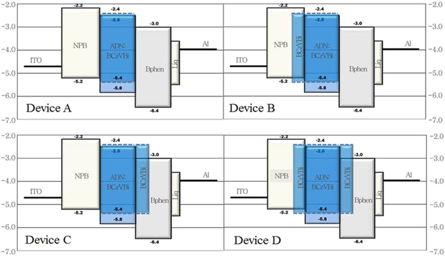
In this Letter, BCzVBi, used for blue fluorescent dopant of EML, was doped in HTL and ETL for fabrication in blue OLED devices. The electrical and optical properties of BCzVBi-doped HTL and ETL on the luminous efficiency of BOLEDs were examined. Figure 1 shows the energy band diagram of blue OLED devices and Table 1 summarizes composition of the devices and layer thicknesses. The effect of different combinations of BCzVBi-doped HTL or ETL or both doped-HTL and ETL on the performance of BOLEDs was investigated.
Sign up for Chinese Optics Letters TOC. Get the latest issue of Chinese Optics Letters delivered right to you!Sign up now
| Device | | HTL | EML | ETL | EIL | metal |
|---|
| A | NPB (700) | | ADN:BCzVBi-7% (300) | | Bphen (300) | Liq (20) | Al (1200) |
| B | NPB (600) | NPB:BCzVBi-7% (100) | ADN:BCzVBi-7% (300) | | Bphen (300) | Liq (20) | Al (1200) |
| C | NPB (700) | | ADN:BCzVBi-7% (300) | Bphen:BCzVBi-7% (100) | Bphen (200) | Liq (20) | Al (1200) |
| D | NPB (600) | NPB:BCzVBi-7% (100) | ADN:BCzVBi-7% (300) | Bphen:BCzVBi-7% (100) | Bphen (200) | Liq (20) | Al (1200) |
Table 1. Layer Structure of Blue OLED Devices (Thickness Unit=Å)

Figure 1.Energy band diagrams of the blue OLED devices A, B, C, and D.
Energy transfer between host molecules and BCzVBi was examined considering the possibility of its charge trapping effect. Eventually, improvement in the luminous efficiency of BOLEDs was achieved through optimizing the layer configuration of theBCzVBi-doped charge transport layer. Blue OLED devices were composed of NPB for HTL, ADN for host material in EML, BCzVBi for the blue dopant in the EML, and Bphen for the ETL. First, we observed the photoluminescence (PL) of NPB, ADN, and Bphen as host materials of BCzVBi and the absorption spectrum of BCzVBi to estimate the energy transfer level between the host and dopant materials. Fig. 2(A) shows the PL and absorption spectra of the organic materials used for the blue OLED. The higher degree of peak overlap between the absorption of the dopant and the PL of the host molecule that happens, the more energy transfer is achieved between BCzVBi and the host materials, such as NPB and Bphen, according to the Forster mechanism[11,12]. The trend of the preferred energy transfer between BCzVBi and a host molecule for the functional materials used in this study is in the order of Bphen, ADN, and NPB, as can be seen in the normalized PL spectra. Generally, energy transfer occurs more efficiently when the overlap between the PL spectrum of the donor and absorption spectrum of the acceptor increases[13]. It is clear that a large overlap between the absorption of BCzVBi and the PL of Bphen is enough to gain more emission.
Figure 3 shows that the ETL-doped device C has a lower luminance than the other devices and this result does not follow the general theory of energy transfer based upon peak overlap. Such a deviation was induced from the normalized PL data and can be explained using the original PL data. Bphen originally had a low intensity of PL and EL, as described in Fig. 2(B), and device C had a lower luminance than device B considering combination with the level of overlap between the original absorption of the host and PL of the dopant. Otherwise, the current density of device C is the highest among blue OLED devices because Bphen has a similar electron mobility of compared with NPB’s hole mobility of [14–16]. The NPB layer is thicker than that of the Bphen layer (300 Å), and it causes an unbalanced electron-hole current in the device. However, BCzVBi acts as an electrical impurity in host materials with high hole and low electron mobilities of and , respectively, measured by the time-of-flight method mentioned in latter part of this Letter[17].
Figure 2.(A) Normalized and (B) original absorption spectrum of BCzVBi with PL spectra of NPB and Bphen.
Figure 3.Plots of (A) current density versus voltage and (B) luminous efficiency versus current density of BOLED devices.
For this reason, BCzVBi was added to Bphen as an ETL to obtain a better charge balance by trapping carriers in the device. However, Bphen does not enhance blue emission, although it has higher current density because of its less exciton generation due to a lower internal quantum efficiency. As a result, BCzVBi cannot receive sufficient energy from Bphen in the ETL and device C has the lowest luminous efficiency among the blue OLED devices in spite of high current density, as shown in Fig. 3(B). Figure 3(B) also shows that the luminous efficiency thatdevice B achieved was 7.24 cd/A at 5 V, which is 18.5% higher than the 6.11 cd/A at 5 V of device A due to the higher level of overlap between NPB and BCzVBi than that of Bphen and BCzVBi, whereas device C only had 5.15 cd/A at 5 V which is 18.6% lower than that of device A. This result explains that BCzVBi forms a trapped energy level in the ETL to inhibit electrons’ drift rendering unbalance of the hole-electron density. Device D doping BCzVBi into both the HTL and ETL showed a similar luminous efficiency due to the cancellation of the constructive and destructive effect of BCzVBi as generating a trapped energy level in the HTL and ETL. As a result of BCzVBi doping into the charged transport layers, the charge balance significantly improves the current density, the emission property, and the peak overlap of the host material influence on their luminance and luminous efficiency.
Figure 4 indicates the electroluminescence (EL) spectra of the blue OLED devices at 6 V. The major and secondary peaks appearing at 449 and 473 nm, obviously formed by BCzVBi[18], indicate that emission occurs in the dopant by Forster energy transfer from host to dopant. Device A and device C have very similar EL spectra. This demonstrates that emission rarely occurs by BCzVBi in the ETL of Bphen. Also, the peak of 473 nm shows that various intensities by the BCzVBi doping position and the EL intensity of device B are higher than other devices, probably due to more favorable energy transfer between the NPB and BCzVBi in the HTL. Finally, we measured the electron mobility of BCzVBi to explain electrical properties of the blue OLED device. The hole mobility of BCzVBi has been previously reported[19]. Figure 5 indicates the time-dependent photocurrent of BCzVBi and field-dependent electron mobility. The mobility is defined by the equation in time of flight[19,20], , where is the thickness of BCzVBi film in this case of 700 nm, t_tran is the transit time, and V is the voltage. The photocurrent shows that the dispersive trend and transit time is defined by the point significantly changing the slope at log-log plot, which is 1.37 μs at 35 V as described in Fig. 5. The field-dependent electron mobility measured for BCzVBi at different voltage and transit times is summarized in Table 2. Figure 5(B) shows that linear relationship between the mobility of BCzVBi and the electric field according to the Poole–Frenkel model, which can explain electron movement from the valance to the conduction band in a high electric field without thermal energy[21].
| Voltage (V) | Time (μs) | Mobility (cm2/Vs) |
|---|
| 25 | 31.40 | 6.24×10⁻⁶ |
| 30 | 20.40 | 8.00×10⁻⁶ |
| 35 | 13.70 | 1.02×10⁻⁵ |
| 40 | 9.79 | 1.25×10⁻⁵ |
| 45 | 8.02 | 1.36×10⁻⁵ |
| 50 | 5.63 | 1.74×10⁻⁵ |
| Hole Mobility of BCzVBi [11] | 1.0×10⁻³ |
Table 2. Calculated Field-Dependent Electron Mobility of BCzVBi
Figure 4.EL spectra of blue OLED devices at 6 V.
Figure 5.(A) Transit time by the photocurrent of BCzVBi at 35 V, and (B) the field dependent mobility of BCzVBi.
In conclusion, improved performance of BOLEDs incorporating the blue fluorescent dopant BCzVBi-doped HTL and ETL is demonstrated. It shows that the luminance and luminous efficiency of BOLEDs made with optimized BCzVBi-doped HTL/EML increase by 22% and 17% as compared to the control BOLEDs with HTL/EML/ETL or HTL/EML/doped-ETL device configurations. As the blue emission is generated only by the BCzVBi dopant, resulting in the CIE color coordinates of (0.15, 0.15), it remains unchanged for the optimal BOLEDs fabricated using doped HTL and ETL. The electron mobility of BCzVBi is estimated to be . Bphen, with high electron mobility, can compensate for the low electron mobility of BCzVBi and eventually enhance electron-hole current balance to improve the luminance and luminous efficiency of BOLEDs. It will be very important to determine the best combination of host and dopant materials to support even more energy transfer and luminous efficiency. This work provides a direction for realizing a better combination of host-dopant systems for the efficient operation of OLEDs.
References
[1] C. W. Tang, S. A. VanSlyke. Appl. Phys. Lett., 51, 913(1987).
[2] Y. Xu, J. Peng, J. Jiang, W. Xu, W. Yang, Y. Cao. Appl. Phys. Lett., 87, 193502(2005).
[3] W. H. Choi, H. L. Tam, F. R. Zhu, D. G. Ma, H. Sasabe, J. Kido. Appl. Phys. Lett., 102, 153308(2013).
[4] C. H. Chen, F. I. Wu, C. F. Shu, C. H. Chien, Y. T. Tao. J. Mater. Chem., 14, 1585(2004).
[5] K. H. Lee, S. O. Kim, K. S. Yook, S. O. Jeon, J. Y. Lee, S. S. Yoon. Synth. Met., 161, 2024(2011).
[6] Y. H. Chen, J. S. Chen, D. G. Ma, D. H. Yan, L. X. Wang, F. R. Zhu. Appl. Phys. Lett., 98, 243309(2011).
[7] L. Wang, Z.-Y. Wu, C. H. Chen. Org. Electron., 12, 595(2011).
[8] J. H. Seo, K. H. Lee, Y. K. Kim. Org. Electron., 11, 1605(2010).
[9] S. R. Forrest. Org. Electron., 4, 45(2003).
[10] P. E. Burrows, S. R. Forrest, S. P. Sibley, M. E. Thompson. Appl. Phys. Lett., 69, 2959(1996).
[11] R. S. Deshpande, V. Bulovic, S. R. Forrest. Appl. Phys. Lett., 75, 888(1999).
[12] S. E. Shaheen, B. Kippelen, N. Peyghambarian. J. Appl. Phys., 85, 7939(1999).
[13] M. Meng, W. Song, Y.-H. Kim, S.-Y. Lee, C. G. Jhun, C.-B. Moon, R. Wood, W.-Y. Kim. Mol. Cryst. Liq. Cryst., 569, 125(2012).
[14] J.-W. Kang, D.-S. Lee, H.-D. Park, Y.-S. Park, J. W. Kim, W.-I. Jeong, K.-M. Yoo, K. Go, S.-H. Kim, J.-J. Kim. J. Mater. Chem., 17, 3714(2007).
[15] J.-W. Kang, S.-H. Lee, H.-D. Park, W.-I. Jeong, K.-M. Yoo, Y.-S. Park, J.-J. Kim. Appl. Phys. Lett., 90, 223508(2007).
[16] J. Littman, P. Martic. J. Appl. Phys., 72, 3610(1992).
[17] C. Hosokawa, H. Tokailin, H. Higashi, T. Kusumoto. Appl. Phys. Lett., 63, 1322(1993).
[18] Y.-H. Kim, W. Y. Kim, C.-B. Moon. J. Appl. Phys., 110, 034501(2011).
[19] S. B. Lee, T. Yasuda, M. J. Yang, K. Fujita, T. Tsutsui. Mol. Cryst. Liq. Cryst., 405, 67(2003).
[20] S. C. Tse, H. H. Fong, S. K. So. J. Appl. Phys., 94, 2033(2003).
[21] J. Frenkel. Phys. Rev., 54, 647(1938).