• Chinese Physics B
  • Vol. 29, Issue 9, (2020)
Jun Wang1、†, Yuquan Wang1, Cong Liu1, Meiling Sun1, Cao Wang1, Guangchao Yin1, Fuchao Jia1, Yannan Mu2, Xiaolin Liu1, and Haibin Yang3
Author Affiliations
  • 1School of Physics and Optoelectronic Engineering, Shandong University of Technology, Zibo 255000, China
  • 2Department of Physics and Chemistry, Heihe University, Heihe 164300, China
  • 3State Key Laboratory of Superhard Materials, Jilin University, Changchun 10012, China
  • show less
    DOI: 10.1088/1674-1056/abad22 Cite this Article
    Jun Wang, Yuquan Wang, Cong Liu, Meiling Sun, Cao Wang, Guangchao Yin, Fuchao Jia, Yannan Mu, Xiaolin Liu, Haibin Yang. Influence of CdS films synthesized by different methods on the photovoltaic performance of CdTe/CdS thin film solar cells[J]. Chinese Physics B, 2020, 29(9): Copy Citation Text show less
    Schematic diagram of the Ni/CdTe/CdS/ITO/Au thin film solar cell.
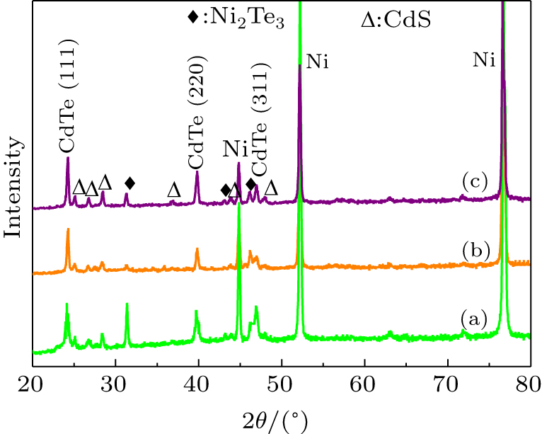
    Fig. 1. Schematic diagram of the Ni/CdTe/CdS/ITO/Au thin film solar cell.
    XRD patterns of the (a) CdTe/CBD-CdS film, (b) CdTe/HP-CdS film, and (d) CdTe/MS-CdS film.
    Fig. 1. XRD patterns of the (a) CdTe/CBD-CdS film, (b) CdTe/HP-CdS film, and (d) CdTe/MS-CdS film.
    Schematic illustration describing the overall process of device fabrication based on CBD-CdS film.
    Fig. 2. Schematic illustration describing the overall process of device fabrication based on CBD-CdS film.
    FESEM images of CdTe/CBD-CdS films with different deposition cycles: (a) 1 cycle and (b) 3 cycles.
    Fig. 2. FESEM images of CdTe/CBD-CdS films with different deposition cycles: (a) 1 cycle and (b) 3 cycles.
    FESEM images of CdTe/HP-CdS films with different deposition cycles: (a) 1 cycle and (b) 3 cycles.
    Fig. 3. FESEM images of CdTe/HP-CdS films with different deposition cycles: (a) 1 cycle and (b) 3 cycles.
    Schematic illustration describing the overall process of device fabrication based on the HP-CdS film.
    Fig. 3. Schematic illustration describing the overall process of device fabrication based on the HP-CdS film.
    Schematic illustration describing the overall process of device fabrication based on the MS-CdS film.
    Fig. 4. Schematic illustration describing the overall process of device fabrication based on the MS-CdS film.
    The cross-section (a) and the top surface (b) FESEM images of CdTe/MS-CdS films.
    Fig. 4. The cross-section (a) and the top surface (b) FESEM images of CdTe/MS-CdS films.
    The J–V curves of (i) CdTe/CBD-CdS solar cell, (ii) CdTe/HP-CdS solar cell, and (iii) CdTe/MS-CdS solar cell.
    Fig. 5. The JV curves of (i) CdTe/CBD-CdS solar cell, (ii) CdTe/HP-CdS solar cell, and (iii) CdTe/MS-CdS solar cell.
    The cross-section (a) and the top surface (b) FESEM images of CdTe/MS-CdS films annealed at 350 °C.
    Fig. 6. The cross-section (a) and the top surface (b) FESEM images of CdTe/MS-CdS films annealed at 350 °C.
    FESEM images of CdTe/CdS films annealed at different temperatures: (a) CdTe/CBD-CdS films annealed at 450 °C, (b) CdTe/HP-CdS films annealed at 450 °C, (c) CdTe/MS-CdS films annealed at 450 °C, (d) CdTe/MS-CdS films annealed at 500 °C.
    Fig. 7. FESEM images of CdTe/CdS films annealed at different temperatures: (a) CdTe/CBD-CdS films annealed at 450 °C, (b) CdTe/HP-CdS films annealed at 450 °C, (c) CdTe/MS-CdS films annealed at 450 °C, (d) CdTe/MS-CdS films annealed at 500 °C.
    SamplesVoc/VJsc/mA ⋅ cm−2FFPCE/%RsRshnJo/mA ⋅ cm−2
    A CdTe/CBD-CdS0.322.710.310.27278.451101.541.122.94 × 10−5
    B CdTe/HP-CdS0.377.000.340.88323.862121.841.213.42 × 10−5
    C CdTe/MS-CdS0.479.510.562.5084.662387.251.232.19 × 10−6
    Table 1. The performance parameters of CdTe thin film solar cells.
    Jun Wang, Yuquan Wang, Cong Liu, Meiling Sun, Cao Wang, Guangchao Yin, Fuchao Jia, Yannan Mu, Xiaolin Liu, Haibin Yang. Influence of CdS films synthesized by different methods on the photovoltaic performance of CdTe/CdS thin film solar cells[J]. Chinese Physics B, 2020, 29(9):
    Download Citation