• Acta Photonica Sinica
  • Vol. 49, Issue 11, 165 (2020)
Xiao-teng LIU1, Ji-jun FENG1、4, Xin-yao WU1, Hai-peng LIU1, Fu-ling ZHANG2, Zhi-hua FENG2, and He-ping ZENG3、4
Author Affiliations
  • 1Shanghai Key Laboratory of Modern Optical System, School of Optoelectronic Information and Computer Engineering, University of Shanghai for Science and Technology, Shanghai200093, China
  • 2The 7th Research Institute of China Electronics Technology Group Corporation, Zhengzhou450047, China
  • 3State Key Laboratory of Precision Spectroscopy Science and Technology, East China Normal University, Shanghai200241, China
  • 4Chongqing Institute of East China Normal University, Chongqing01120, China
  • show less
    DOI: 10.3788/gzxb20204911.1149012 Cite this Article
    Xiao-teng LIU, Ji-jun FENG, Xin-yao WU, Hai-peng LIU, Fu-ling ZHANG, Zhi-hua FENG, He-ping ZENG. Silicon Waveguide Based Integrated Optical Phased Array Chips (Invited)[J]. Acta Photonica Sinica, 2020, 49(11): 165 Copy Citation Text show less
    Waveguide cross-sectional mode distribution
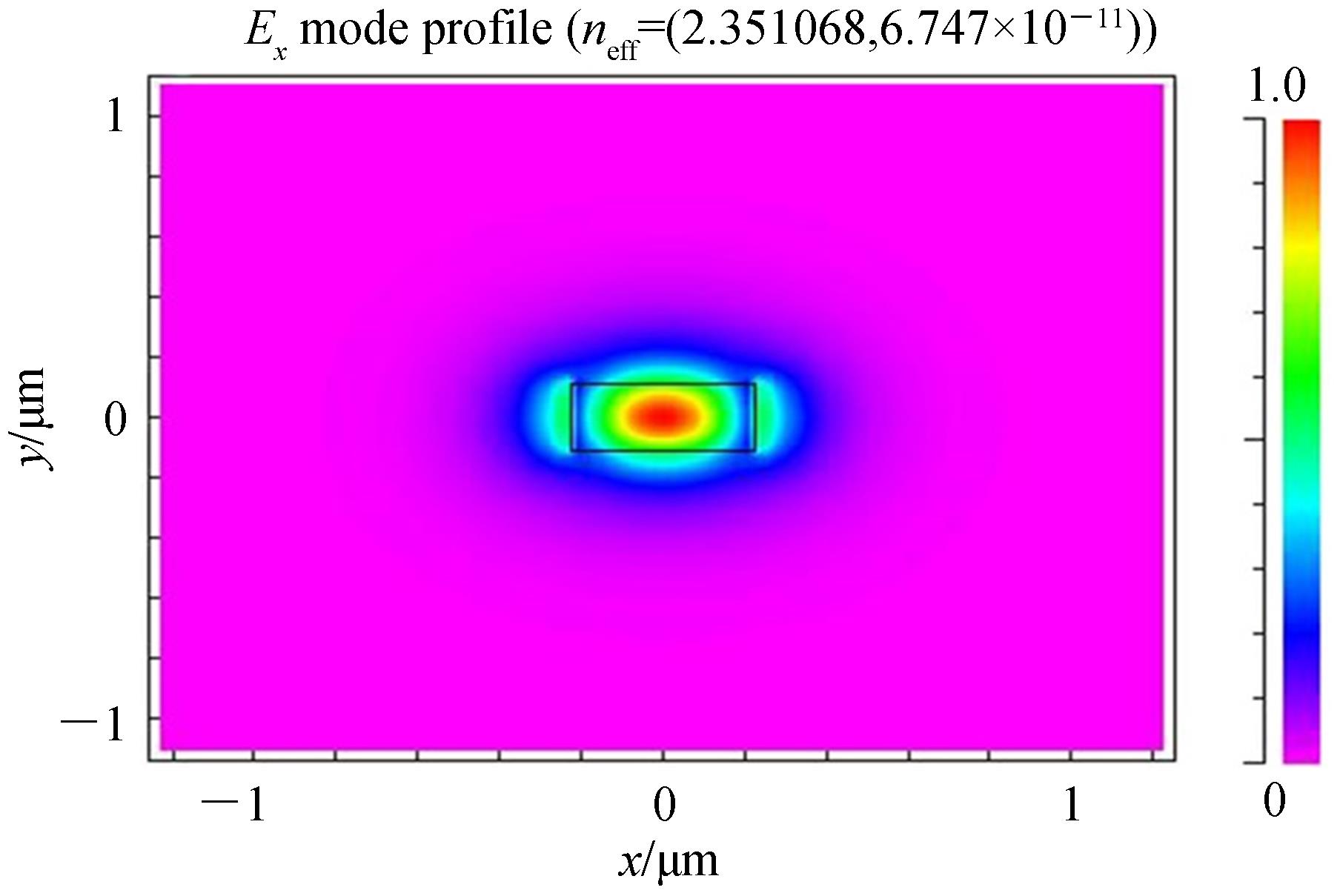
    Fig. 1. Waveguide cross-sectional mode distribution
    The relationship between array waveguide coupling crosstalk and waveguide length
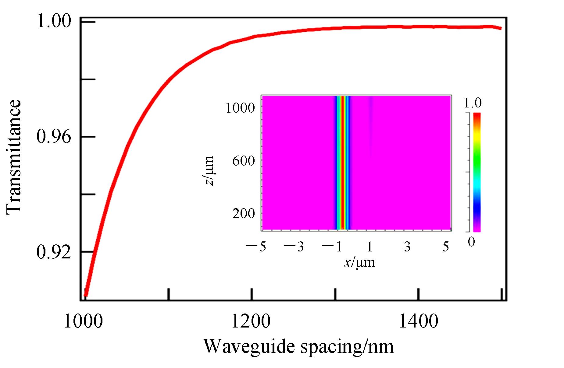
    Fig. 2. The relationship between array waveguide coupling crosstalk and waveguide length
    Light field distribution of beam splitter
    Fig. 3. Light field distribution of beam splitter
    The relationship between beam splitter transmittance and wavelength
    Fig. 4. The relationship between beam splitter transmittance and wavelength
    The relationship between the mode equivalent refractive and the effective refractive index of the waveguide core
    Fig. 5. The relationship between the mode equivalent refractive and the effective refractive index of the waveguide core
    The relationship between the FWHM of far-field spot divergence angle and the number of arrayed waveguides
    Fig. 6. The relationship between the FWHM of far-field spot divergence angle and the number of arrayed waveguides
    Array waveguide far-field spot deflection simulation
    Fig. 7. Array waveguide far-field spot deflection simulation
    Flow chart of silicon-based phased array chip preparation
    Fig. 8. Flow chart of silicon-based phased array chip preparation
    Preparation of silicon-based phased array chip and packaging effect
    Fig. 9. Preparation of silicon-based phased array chip and packaging effect
    Schematic diagram of measurement system
    Fig. 10. Schematic diagram of measurement system
    The far-field spot before and after optimization by particle swarm optimization
    Fig. 11. The far-field spot before and after optimization by particle swarm optimization
    The effect of spot deflection with different phase-shifting voltages applied
    Fig. 12. The effect of spot deflection with different phase-shifting voltages applied
    The effect of spot deflection under 1550~1610 nm wavelength tuning
    Fig. 13. The effect of spot deflection under 1550~1610 nm wavelength tuning
    Xiao-teng LIU, Ji-jun FENG, Xin-yao WU, Hai-peng LIU, Fu-ling ZHANG, Zhi-hua FENG, He-ping ZENG. Silicon Waveguide Based Integrated Optical Phased Array Chips (Invited)[J]. Acta Photonica Sinica, 2020, 49(11): 165
    Download Citation