• Chinese Optics Letters
  • Vol. 18, Issue 9, 090602 (2020)
Shaowen Lu1、2、3、*, Yu Zhou1, Funan Zhu2、3, Jianfeng Sun1、2, Yan Yang3, Ren Zhu3, Shengnan Hu3, Xiaoxi Zhang3, Xiaolei Zhu1、2, Xia Hou2、3、**, and Weibiao Chen1、2
Author Affiliations
  • 1Key Laboratory of Space Laser Communication and Detection Technology, Shanghai Institute of Optics and Fine Mechanics, Chinese Academy of Sciences, Shanghai 201800, China
  • 2Center of Materials Science and Optoelectronics Engineering, University of Chinese Academy of Sciences, Beijing 100049, China
  • 3Laboratory of Space Laser Engineering, Shanghai Institute of Optics and Fine Mechanics, Chinese Academy of Sciences, Shanghai 201800, China
  • show less
    DOI: 10.3788/COL202018.090602 Cite this Article Set citation alerts
    Shaowen Lu, Yu Zhou, Funan Zhu, Jianfeng Sun, Yan Yang, Ren Zhu, Shengnan Hu, Xiaoxi Zhang, Xiaolei Zhu, Xia Hou, Weibiao Chen. Digital-analog hybrid optical phase-lock loop for optical quadrature phase-shift keying[J]. Chinese Optics Letters, 2020, 18(9): 090602 Copy Citation Text show less

    Abstract

    We analyze a feasible high-sensitivity homodyne coherent optical receiver for demodulating optical quadrature phase-shift keying (QPSK). A fourth-power phase-lock loop based on a digital look-up table is used. Considering the non-negligible loop delay, we optimize the loop natural frequency. Without error correction coding, a sensitivity of ?37 dBm/?35 dBm is achieved, while the bit error rate is below 10?9 at 2.5 Gbaud/5 Gbaud rate. For the QPSK communication system, the bit rate is twice the baud rate. The loop natural frequency is 0.647 Mrad/s, and the minimized steady-state phase-error standard deviation is 3.83°.

    For the digital coherent optical communication system, the receiver samples the analog electrical signals through a high-speed analog-to-digital converter (ADC). In general, the bandwidth of the electrical signal is equal to the baud rate. According to the Nyquist sampling theorem, the sampling rate of the ADC is twice the baud rate. The digital signal processor recovers the digital baseband signal based on the frequency offset estimation algorithm and carrier phase recovery algorithm[1]. With the increasing of the communication rate, the sampling rate of the ADC and the digital signal processor are challenged[2]. At the same time, the power consumption of the receiver will increase[3].

    The homodyne coherent receiver based on optical phase-lock loop (OPLL) has attracted attention due to its low power consumption. The losses caused by the receiver can be compensated by an erbium-doped fiber amplifier (EDFA)[4]. Compared with binary phase-shift keying (BPSK), the quadrature phase-shift keying (QPSK) can carry 2 bits of information per symbol[5]. In 2002, Griffin et al. studied the optical differential QPSK (oDQPSK). The signal is demodulated by using an optical delay-and-add structure and is easier to realize than a homodyne coherent receiver[6]. However, the differential demodulation scheme suffers from a sensitivity penalty of about 2.3 dB compared with the ideal sensitivity of coherent QPSK detection[7]. In 2006, Pfau et al. reported the real-time synchronous QPSK transmission and digital in-phase quadrature (IQ) receiver. A 400 Mbaud QPSK data was transmitted quasi-error-free in a self-homodyne configuraton[8]. For an ideal shot-noise limited optical QPSK homodyne/heterodyne detection, the quantum limit of sensitivity for a 109 bit error rate (BER) is 36 photons persymbol (18 photons/bit) and has an intrinsic 3 dB penalty compared with homodyne BPSK detection, equaling the sensitivity of heterodyne BPSK detection[9].

    For the multi-gigabit QPSK receiver based on OPLL, it is difficult to extract the phase-error signal and the coefficient setting of the OPLL[10]. In 1992, Norimatsu et al. adopted the decision-directed phase-lock loop (PLL), and the phase-error signal was extracted by using digital exclusive OR (EX-OR) circuits instead of analog circuits[11]. But, this OPLL scheme generates the four-fold phase error and offers 90° phase ambiguity, which needs to be eliminated by differential encoding. In 2014, Fujii et al. reported QPSK demodulation based on digital OPLL[12]. The phase-error signal was extracted by a track and hold (T&H) circuit and a field-programmable gate array (FPGA). A second-order active loop filter was used and had a better phase margin. However, compared with the first-order active loop filter, the complexity of the coefficient setting is greatly increased.

    In this Letter, the fourth-power phase-lock algorithm based on an FPGA is presented. The first-order active filter is used as a loop filter. This scheme is applicable to M-array phase-shift keying (PSK) and quadrature amplitude modulation (QAM) signals by changing the relevant digital processing algorithm. The performance of a QPSK homodyne coherent receiver is examined. The Padé approximation is adopted in calculation of the phase-error variance with the non-negligible loop propagation delay, and the loop natural frequency is optimized.
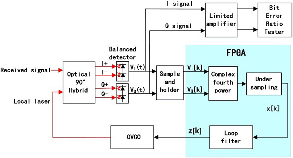
    First of all, Fig. 1 shows the structure of the QPSK homodyne coherent receiver. The optical 90° hybrid combines the received signal laser with the local laser and outputs two arms (I-arm and Q-arm), maintaining the phase differences of the output signal at 90° or 180°. The output voltages of the I-arm and Q-arm are expressed as where k is the power splitting ratio of the optical 90° hybrid to the Q-arm and equal to 0.5 for QPSK; R and RL are the detector’s responsivity and load resistance; PS and PL are the received signal power and local laser power; φn(t) represents the carrier phase noise; φL(t) represents the phase of the local laser controlled by OPLL; θ(t)(=0,π/2,π,3π/2) is the QPSK phase modulation; nI(t) and nQ(t) are the shot-noise processes for the I-arm and Q-arm.

    Schematic of the QPSK fourth-power phase-lock loop.

    Figure 1.Schematic of the QPSK fourth-power phase-lock loop.

    VI(t) and VQ(t), the two analog signals, are sampled and quantized synchronously by an ADC with a sampling rate of 125 MHz. In order to remove the modulated signal and recover the phase-error signal, the digitalized signals are input into the normalized complex fourth-power look-up table implemented in FPGA. The function of the normalized complex fourth-power look-up table follows Im{·} represents the imaginary part of the normalized complex signal. According to Eqs. (1) and (2), there is ej4θ[k]=1 for all time. Eq. (3) can be expressed as

    To simplify the analysis, we assume that the loop remains in lock with a small phase error,

    Equation (5) can be linearized using the approximation sinxx, where x[k] is the phase-error signal of the phase-lock loop; n[k] represents the shot noise and is modeled as a zero-mean random truncated Gaussian-type distribution[13]. After passing through the loop filter realized by the proportional-integral digital control algorithm, the output signal is z[k].

    We investigate the functionality of an optical voltage controlled oscillator (OVCO). As shown in Fig. 2, the direct digital synthesizer (DDS) generates the corresponding sinusoidal signal according to the signal z[k], and the frequency of the sinusoidal signal fDDS is expressed as where fc is the working clock of the DDS and equals 125 MHz; N is the word length of the DDS phase accumulator word and is equal to 32. The function of the electrical mixer is a frequency adder and outputs a sinusoidal signal whose frequency is the sum of sinusoidal signal fDDS and RF signal fRF. The output of the electrical mixer drives the phase modulator and produces an optical sideband series. An optical filter is used to obtain the +1-order sideband of the optical sideband series. The optical frequency of the +1-order sideband used as a local laser is fLO+fDDS+fRF. The side-mode suppression ratio (SMSR) reaches 40 dB. As fDDS is controlled by the feedback PLL, the lower input signal of the 90° hybrid will lock to the received signal.

    Principle of electro-optic modulation frequency shift as OVCO.

    Figure 2.Principle of electro-optic modulation frequency shift as OVCO.

    Next, we introduce the linear model diagram of an analog optical QPSK fourth-power PLL, as shown in Fig. 3. The phase-error signal is extracted from the carrier phase noise φn(t) and local laser phase φL(t), and a white noise n(t) is added. τ represents the total delay of the loop. In our experiment, the loop filter adopts a first-order active filter, and the transfer function is F(j2πf)=(1+j2πfτ2)/j2πfτ1. In order to improve the accuracy and stability of the PLL, the lead phase compensation algorithm (LPCA) based on a soft phase compensator is added. Finally, it integrates to generate the control phase φL(t). The loop filter is replaced by a digital control algorithm implemented in FPGA.

    Linear model of the analog fourth-power OPLL.

    Figure 3.Linear model of the analog fourth-power OPLL.

    According to Fig. 3, the closed-loop transfer function of the OPLL can be expressed as where KPD and KVCO are the gain of the detector and the OVCO; ωn and ζ are the natural frequency and damping factor of the PLL.

    The single sided power spectral densities (PSDs) of the phase noise SPN(f) caused from φn(t) and of the shot noise SSN(f) caused from n(t) are expressed as Δν represents the total linewidth of the signal laser and local laser; Ka is the coefficient of the 1/f noise; e is the electron charge. In the condition that the phase noise and shot-noise processes are independent from each other, the variance σ2 of the steady-state phase error has already been obtained as

    In order to get the analytic solution, one method is using the Padé approximation[14]. The (2,2)th Padé approximation of ea is given by

    According to the (2,2)th Padé approximation with the damping factor, ζ is set to be 0.707, and Eq. (13) can be expressed as where y=τ/τ2; σPN2 and σSN2 are the variance of the steady-state phase error caused by phase noise and shot noise, respectively. According to the analysis of Norimatsu et al.[15], the (2,2)th Padé approximation is in good agreement with the exact numerical solution when ωnτ is less than 0.6.

    Now, we optimize the loop parameters. Table 1 is the experimental parameters. According to Table 1 and Eqs. (10)–(15), Fig. 4 illustrates the relationship between the phase-error standard deviation σ and the loop natural frequency ωn under the different loop delays. The effects of the loop delay have two aspects: first, the increased delay time reduces the optimal natural frequency; second, the increased delay time increases the resulting minimized steady-state phase-error variance.

    ParameterSymbolValue
    Laser wavelengthλ1549.72 nm
    Received signal powerPs−45 to 35dBm
    Communication rateRb10 Gbps
    Linewidth (TX/RX)Δν300 Hz
    ResponsivityR0.85 A/W
    Power-splitting ratioK0.5

    Table 1. Experimental Parameters

    Phase-error standard deviation versus loop natural frequency.

    Figure 4.Phase-error standard deviation versus loop natural frequency.

    The optimized natural frequency under specific loop delay τ is shown in Fig. 5. According to the fitted curve, the optimal value is found to be

    Optimized natural frequency versus loop delay time.

    Figure 5.Optimized natural frequency versus loop delay time.

    The increase of the loop delay τ will reduce the natural frequency ωn. In order to reduce the effect of loop delay τ, the LPCA is used. The principle of LPCA is to average the signal z[k] eight times and then input the averaged signal to the interface of the DDS’s phase control word. It will generate the corresponding phase compensation.

    According to the above analysis, the variance σ2 of the steady-state phase error is related to the linewidth of the laser. In general, the single sided PSD of frequency fluctuation Sv(f) can be tested by the instrument. Sv(f) can be expressed as

    Figure 6(a) is the PSD of frequency fluctuation Sv(f) tested from the laboratory. When the frequency is high (higher than 100 kHz), the 1/f noise is very small and can be ignored. It can be seen from the Fig. 6(a) that the convergent value of Sv(f) is 100Hz2/Hz, and the corresponding laser linewidth is 300 Hz. Figure 6(b) shows the received signal constellations. The error vector magnitude (EVM) is 9.34% and is accurate enough for the receiver to achieve the specified reception performance.

    (a) Frequency fluctuation PSD of the transmitter (TX)/receiver (RX) laser and (b) the constellation of the QPSK modulation signal.

    Figure 6.(a) Frequency fluctuation PSD of the transmitter (TX)/receiver (RX) laser and (b) the constellation of the QPSK modulation signal.

    We built a QPSK homodyne coherent receiver based on the fourth-power OPLL. The performance of the OPLL is verified by simulation and experiment. In our experiment, the detector model is KPDX10G. The ADC model is EV10AQ190A. The series of the FPGA used in the experiments is xc7k420tffg901-2. ADC sampling delay is 69 ns; FPGA algorithm computing delay is 112 ns; digital-to-analog converter (DAC) delay (restricted by the hardware) is 338 ns, and the fiber delay is about 6 ns. The total loop delay is 525 ns. According to Eq. (16), the corresponding optimal natural frequency is 0.647 Mrad/s, and the minimized steady-state phase-error standard deviation is 3.83°. Table 2 shows the specification list of the FPGA.

    NameParameter
    Fourth-power look-up tableInput bitwidth: 7 bitOutput bitwidth: 10 bit
    First-order active loop filterInput bitwidth: 10 bitOutput bitwidth: 32 bit
    Direct digital synthesizerPhase accumulator word: 32Output bitwidth: 16 bit
    Working clock125 MHz

    Table 2. Specification List about FPGA

    In order to understand the signal form of each step in the OPLL algorithm, Fig. 7 shows the results of the simulation. Figure 7(a) is the original IQ signal sampled by ADC. The QPSK phase modulation signal θ(t) is removed after the normalized complex fourth power. There are frequency offset and phase difference, as shown in Fig. 7(b). When the OPLL works, the corresponding phase-error signal is as shown in Fig. 7(c). Figure 7(d) is the constellation of the recovered IQ signal.

    QPSK fourth-power phase-lock loop simulation: (a) the Lissajous of the original signal sampled by 125 MSa/s; (b) the fourth power of the original signal; (c) phase error of the phase-locked state; (d) the constellation of the recovered IQ signal.

    Figure 7.QPSK fourth-power phase-lock loop simulation: (a) the Lissajous of the original signal sampled by 125 MSa/s; (b) the fourth power of the original signal; (c) phase error of the phase-locked state; (d) the constellation of the recovered IQ signal.

    We further analyze the sensitivity of the QPSK homodyne coherent receiver system, where the BER is affected by the signal-to-noise ratio (SNR) and phase-error variance. The probability of bit error is obtained by Rhodes as[16]Rb is the bit rate. The erfc(x) is a Gaussian error function defined as

    Prabhu has presented the sensitivity loss caused by phase-locked error. For a QPSK homodyne coherent detection, standard deviations of σ=2.97° and σ=3.78° correspond to power penalties of 0.5 dB and 1 dB at 109 BER, respectively[17].

    We measured the back-to-back BER of the QPSK communication receiver. Figure 8 shows the BER with respect to the received signal power for 2.5 Gbaud and 5 Gbaud QPSK. The received signal power threshold for a 109 BER reaches 37dBm/35dBm in the case of 2.5 Gbaud and 5 Gbaud. Comparing to the quantum limitation, there is about 12 dB penalty. This penalty is mainly caused by the noise factor of EDFA (4 dB), the bandwidth of the balanced photodetector 10 GHz which contributes to 3 dB penalty, and the residual phase error of OPLL (2 dB). The remaining 3 dB penalty is from other factors; for example, the signal quality of the transmitter and the fiber connector.

    BER versus received signal power for 2.5 Gbaud/5 Gbaud.

    Figure 8.BER versus received signal power for 2.5 Gbaud/5 Gbaud.

    In summary, a homodyne coherent optical receiver for demodulating 2.5 Gbaud/5 Gbaud QPSK has been studied. By means of digital-analog hybrid PLL, the requirements of bandwidth of PLL electronics and sampling rate are reduced. The phase-error signal is extracted by a fourth-power PLL. Through simulation and experiments, we have optimized the loop natural frequency under the non-negligible loop propagation delay. The receiving sensitivity reaches 37dBm/35dBm at bit rate of 2.5 Gbaud/5 Gbaud. By the LPCA, the accuracy of phase lock and stability of the receiver are improved, which is of great significance for the realization of higher-speed, high-sensitivity coherent optical communication systems. Improved results can be easily obtained by reducing the total loop delay and optimizing the performance of the detector. They would relax the requirement for laser linewidth and reduce the steady-state phase error of the PLL.

    References

    [1] D. S. Ly-Gagnon, S. Tsukamoto, K. Katoh, K. Kikuchi. J. Lightwave Technol., 24, 12(2006).

    [2] O. Adamczyk, R. Noe2008 Digest of the IEEE/LEOS Summer Topical Meetings, 119(2008).

    [3] E. Torrengo, V. Ferrero, S. Camatel. IEEE Photon. Technol. Lett, 21, 1296(2009).

    [4] M. Z. Amin, K. K. Qureshi, M. M. Hossain. Chin. Opt. Lett., 17, 010602(2019).

    [5] J. S. Hu, Z. C. Zhang, L. Wu, J. Dang, G. H. Zhu. Chin. Opt. Lett., 16, 120101(2018).

    [6] R. A. Griffin, A. C. CarterOptical Fiber Communication Conference and Exhibit, 367(2002).

    [7] D. S. Ly-Gagnon, K. Katoh, K. Kikuchi. Electron. Lett., 41, 206(2005).

    [8] T. Pfau, S. Hoffmann, R. Peveling, S. Bhandare, S. K. Ibrahim, O. Adamczyk, M. Porrmann, R. Noé, Y. AchiamOptical Amplifiers and Their Applications/Coherent Optical Technologies and Applications(2006).

    [9] F. Derr. J. Lightwave Technol., 10, 1290(1992).

    [10] H. Zhongxia, D. Kuykenstierna, L. Szhau, H. Zirath2015 IEEE MTT-S International Microwave Symposium, 1(2015).

    [11] S. Norimatsu, K. Iwashita, K. Noguchi. IEEE Photon. Technol. Lett, 4, 765(1992).

    [12] A. Fujii, F. Shirazawa, Y. Kanda, H. Murai. IEEE Photon. Technol. Lett, 26, 1847(2014).

    [13] V. K. Prabhu. IEEE Trans. Aerosp. Electron. Syst., AES-12, 275(1976).

    [14] S. Norimatsu, K. Iwashita. J. Lightwave Technol., 9, 1367(1991).

    [15] S. Norimatsu, K. Iwashita. J. Lightwave Technol., 10, 341(1992).

    [16] S. A. Rhodes. IEEE Trans. Commun., 22, 1046(1974).

    [17] J. R. Barry, J. M. Kahn. J. Lightwave Technol., 10, 1939(1992).

    Shaowen Lu, Yu Zhou, Funan Zhu, Jianfeng Sun, Yan Yang, Ren Zhu, Shengnan Hu, Xiaoxi Zhang, Xiaolei Zhu, Xia Hou, Weibiao Chen. Digital-analog hybrid optical phase-lock loop for optical quadrature phase-shift keying[J]. Chinese Optics Letters, 2020, 18(9): 090602
    Download Citation