The recent advancement in thin film lithium niobate photonic integration technology has been rapid, driven by profound physical, material, and technological factors. Single crystal thin film lithium niobate is particularly noteworthy for offering the most comprehensive performance solution to date, addressing long-term challenges in low transmission loss, high-density integration, and low modulation power consumption within the realm of photonic integrated circuits. This paper provides an overview of the origin and recent swift development of thin film lithium niobate photonic technology, focusing on its potential for the future generation of high-speed optoelectronic devices and ultra-large-scale photonic integrated circuit applications. Various processing technologies for thin film lithium niobate photonic structures are discussed, accompanied by the introduction of current high-performance devices and systems. These include ultra-low loss tunable optical delay lines, ultra-fast light modulators, high-efficiency quantum light sources, as well as high-power on-chip amplifiers and lasers. These devices, distinguished by their unprecedented advantages of small size, light weight, low power consumption, and high performance, are poised to make a tremendous impact on the entire optoelectronic industry.
Since the laboratory production of the lithium niobate single crystal, lithium niobate has emerged as a crucial material in the fields of electro-optics and nonlinear optics. Optical modulators based on the linear electro-optic effect, utilizing lithium niobate, offer notable advantages including high modulation rates, a substantial extinction ratio, low chirp, and high linearity. In the 21st century, integrated photonics technology has gained increasing attention for two primary reasons. Firstly, the demand for photonic devices with attributes such as low energy consumption, high-performance computing, and reconfiguration capabilities has surged due to the explosive growth in applications for information technology, including big data, artificial intelligence, high-speed networks, virtual reality, and quantum information processing. Secondly, integrated photonics technology itself has been continuously advancing. The enhancement of on-chip photonic device performance and cost reduction have reached a threshold that is propelling the emergence of a new photonic industry.
Traditional fabrication techniques, such as ion diffusion and ion implantation, impose limitations on the modulation efficiency and power consumption of lithium niobate modulators, impeding the progress of lithium niobate photonic integration technology. Overcoming this challenge requires addressing both material platforms and device fabrication. In this context, thin film lithium niobate has emerged as a pivotal material, paving the way for integrated photonics. China has long been engaged in research on lithium niobate materials and photonics, contributing significantly to the field's advancement through several crucial milestones. Therefore, it is essential to summarize the recent revolution to provide guidance for future development.
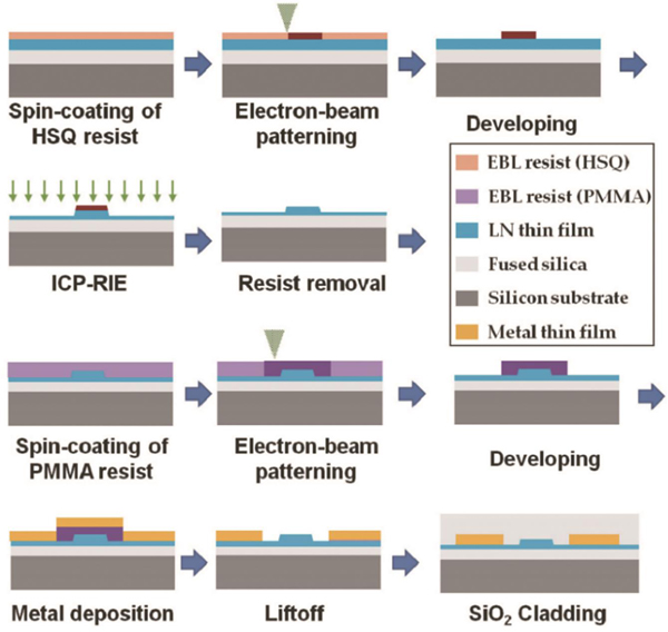
The fabrication flow diagram for the electron beam lithography combined with ion etching process is presented (Fig. 1). A schematic diagram of the photolithography-assisted chemo-mechanical etching (PLACE) technique is provided (Fig. 2). The report includes an ultra-high-speed high-resolution laser lithography system for lithium niobate integrated photonics (Fig. 3). Through the integration of thin film lithium niobate with advanced fabrication techniques, substantial progress has been achieved in the development of lithium niobate photonic devices, encompassing delay lines (Fig. 4), high-speed electro-optical modulators (Fig. 5), optical frequency combs (Fig. 6), quantum light sources (Fig. 7), metasurfaces (Fig. 8), waveguide lasers (Fig. 9), and amplifiers (Fig. 10). Additionally, the article outlines some integrated photonics applications. Specifically, the achievement of electro-optically 4×4 programmable photonic circuits enabled by wafer-scale integration on thin film lithium niobate is illustrated (Fig. 11). This device, composed of cascaded MZIs, demonstrates a total on-chip power dissipation of only 1.5 mW when operated at a 100 MHz modulation rate. Furthermore, an on-chip arrayed waveguide grating (AWG) fabricated on thin film lithium niobate with on-chip loss as low as 3.32 dB is reported (Fig. 12). Finally, four-channel waveguide amplifiers fabricated on monolithically integrated active/passive thin film lithium niobate are also showcased (Fig. 11), demonstrating a robust low-loss optical interface for the monolithic integration of passive and active thin film lithium niobate photonics.
Significant enhancements have been achieved in critical parameters of photonic devices, including modulation bandwidth, power consumption, propagation loss, and active and passive functionalities, as well as advancements in large-scale integration. These technological strides are poised to benefit the evolution of integrated photonics applications. However, some exceptional performances have yet to reach the physical limits of lithium niobate photonics devices, necessitating further efforts in thin film lithium niobate integrated photonics technology. Notably, numerous thin film lithium niobate photonics devices have already approached or even attained optical performances suitable for industrial applications. This opens up abundant opportunities for the development of next-generation optical information technology.