
Yanhui Hou, Teng Zhang, Jiatao Sun, Liwei Liu, Yugui Yao, Yeliang Wang. Progress on 2D topological insulators and potential applications in electronic devices[J]. Chinese Physics B, 2020, 29(9):
- Chinese Physics B
- Vol. 29, Issue 9, (2020)
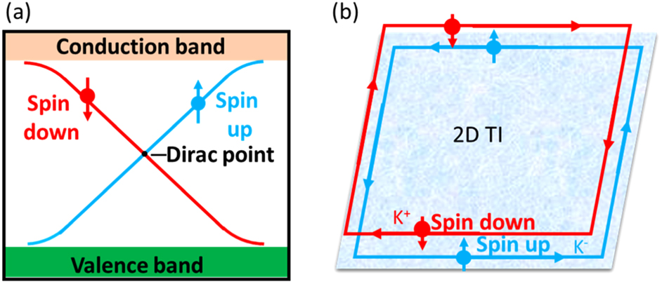
Fig. 1. (a) Band structure of 2DTI, which has the gap in the bulk denoted by the separation between conduction band and valence band, and gapless states at the edge denoted by the blue and red curves. The blue and red branches carry spin up and down currents, respectively. (b) Spin–momentum locking in the edge states of 2DTI in real space.
![(a) Calculated electronic band structures of buckled silicene and germanene. (b) Band structures of silicene or germanene under different vertical electric field E, which turns a topological insulator to a band insulator. (c) Schematic model of dual-gated silicene FET. (a) Reprinted with permission from Ref. [23]. Copyright 2011, American Physical Society. (b) Adopted with permission from Ref. [38]. (c) Reprinted with permission from Ref. [39]. Copyright 2012, American Chemical Society.](/richHtml/cpb/2020/29/9/097304/img_2.jpg)
Fig. 2. (a) Calculated electronic band structures of buckled silicene and germanene. (b) Band structures of silicene or germanene under different vertical electric field E , which turns a topological insulator to a band insulator. (c) Schematic model of dual-gated silicene FET. (a) Reprinted with permission from Ref. [23 ]. Copyright 2011, American Physical Society. (b) Adopted with permission from Ref. [38 ]. (c) Reprinted with permission from Ref. [39 ]. Copyright 2012, American Chemical Society.
Fig. 3. Geometric and electronic structures of silicene and germanene. (a) STM image, theoretical simulated image, and crystal structure of silicene on Ir(111) from left to right. (b) STM image of buckled germanene on Pt(111). (c) T and H phases of silicene on Ag(111) substrate. (d) STM images of silicene nanoflake intercalated between graphene and Ru(0001). (e) Calculated electronic localization function (ELF), showing the covalent interaction existing between adjacent germanium atoms and electrostatic interaction between germanium atom and substrate. (f) dI /dV on monolayer (red) and bilayer (black) germanene. (g) dI /dV mapping on the 2nd layer silicene island which can derive the linear dispersion relationship of Dirac fermion. (h) Splitting of Dirac cone observed by angle resolved photoemission (ARPES) on 3 × 3-silicene on Ag(111). (a) Reprinted with permission from Ref. [40 ]. Copyright 2014, WILEY-VCH Verlag GmbH & Co. KGaA, Weinheim. (c) Reprinted with permission from Ref. [41 ]. Copyright 2012, American Chemical Society. (d) Reprinted with permission from Ref. [42 ]. Copyright 2018, WILEY-VCH Verlag GmbH & Co. KGaA, Weinheim. (f) Reprinted with permission from Ref. [43 ]. Copyright 2017, WILEY-VCH Verlag GmbH & Co. KGaA, Weinheim. (g) Reprinted with permission from Ref. [44 ]. Copyright 2012, American Physical Society. (h) Reprinted with permission from Ref. [45 ]. Copyright 2019, American Physical Society.
Fig. 4. Geometric and electronic structures of antimony monolayer. (a) Atomic structures of the buckled and flat honeycombs of antimony. (b), (c) Atomic resolution STM image of the buckled antimonene monolayer (BAM) and flat antimonene monolayer (FAM). Inset: line profile corresponding to the line in panel. (d) Band structures and the edge states of antimony monolayer. FAM has a topologically nontrivial edge state and BAM has a topologically trivial edge state. Red lines denote the edge states. (e) Inverted band of antimony monolayer induced by increasing strain field. (f) Edge states of antimonene island on top of ML antimonene. (g) STM image and dI /dV mapping of the antimonene island. (a), (c), (d) Reprinted with permission from Ref. [50 ]. Copyright 2018, American Chemical Society. (b) Reprinted with permission from Ref. [51 ]. Copyright 2017, WILEY-VCH Verlag GmbH & Co. KGaA, Weinheim. (e) Reprinted with permission from Ref. [14 ]. Copyright 2015, Nature Publishing Group. (f), (g) Reprinted with permission from Ref. [52 ]. Copyright 2019, American Chemical Society.
Fig. 5. Geometric and electronic structures of bismuthene and BiX layers. (a) Sketch of a bismuthene layer placed on the threefold-symmetric SiC(0001) substrate. (b) DFT calculated electronic band structures and ARPES experimental electronic band dispersion of single layer bismuthene. (c) Spatially resolved dI /dV data across the step, the dI /dV signal of the in-gap states/peaks at the edges of bismuthene film. (d) Atomic structure of monolayer BiX /SbX (X = H, F, Cl, Br), by top view and side view. (e) Electronic band structure of BiH and BiF with large gap. Red line means SOC is considered, but the gray line is not. (f) Side view and top view of the crystal structure of single-layer Bi4Br4. (g) The edge state and spin polarization of different layers of Bi4Br4. The layer dependence of energy gap of few-layer Bi4Br4 (left panel), and band structures of single-layer and triple-layer Bi4Br4 (right panel). (a)–(c) Reprinted with permission from Ref. [60 ]. Copyright 2017, American Association for the Advancement of Science. (d), (e) Reprinted with permission from Ref. [61 ]. Copyright 2014, Nature Publishing Group. (f), (g) Reprinted with permission from Ref. [62 ].
Fig. 6. Geometric and electronic structures of TMDs. (a) Three typical atomic configurations of transition metal dichalcogenides (TMDs, MX 2). (b) Band inversion of 1T′-MX 2 induced by vertical electric fields. (c) A vdW-FET by stacking several layers of 1T′-MX 2 and 2D dielectric layers (h-BN). (d) Experimental dI /dV map taken at the 1T′–1H interface. (e) Atomic resolution STM image of the single-layer 1T′-WTe2 surface and dI /dV fitted with a linear function near the Fermi energy. (f) Pseudo 3D image of WTe2 showing a step edge and the calculated topological edge state of the monolayer 1T′-WTe2 bulk electronic structure. (a)–(c) Reprinted with permission from Ref. [63 ]. Copyright 2014, American Association for the Advancement of Science. (d) Reprinted with permission from Ref. [64 ]. Copyright 2018, Nature Publishing Group. (e) Reprinted with permission from Ref. [65 ]. Copyright 2018, Nature Publishing Group. (f) Reprinted with permission from Ref. [66 ]. Copyright 2017, Nature Publishing Group.
Fig. 7. Quasi-2D topological materials and the optoelectronic coupling. (a) Crystal structure and ARPES images of Bi2Te3. (b) ARPES image and schematic of infrared laser pump excited electrons from the valence band (orange) into the conduction band of Bi2Te3. (c) Crystal structure of the type-II WSM TaIrTe4 and broadband photoresponse of TaIrTe4 photodetector. (d) Schematics of photocurrent generations in type I (left panel) and type II (right panel) Weyl systems. (a) Reprinted from Ref. [73 ]. Copyright 2009, American Association for the Advancement of Science. (b) Reprinted with permission from Ref. [74 ]. Copyright 2012, American Chemical Society. (c) Reprinted with permission from Ref. [75 ]. Copyright 2018, American Chemical Society. (d) Reprinted with permission from Ref. [76 ]. Copyright 2017, American Physical Society.
|
Table 1. The values of SOC gap in different 2DTI.


Set citation alerts for the article
Please enter your email address

© Copyright 2018-2021 | Chinese Laser Press. All Rights Reserved 沪ICP备15018463号-20