
Hui Wang, Deliang Zhou, Yan Wang, Runfeng Su, Shaohe Li, Xuecou Tu, Xiaoqing Jia, Lin Kang, Biaobing Jin, Huabing Wang, Jian Chen, Peiheng Wu. Simulation for embedded-defects foam terahertz images of active bifocal terahertz imaging system at 0.22 THz based on geometric optics[J]. Chinese Optics Letters, 2023, 21(6): 061102
- Chinese Optics Letters
- Vol. 21, Issue 6, 061102 (2023)
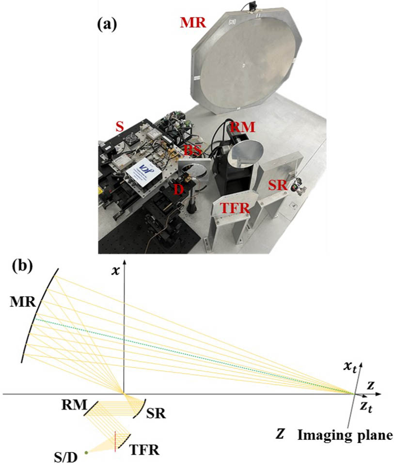
Fig. 1. (a) Photograph of the active bifocal THz imaging system; (b) 2D schematic of imaging.
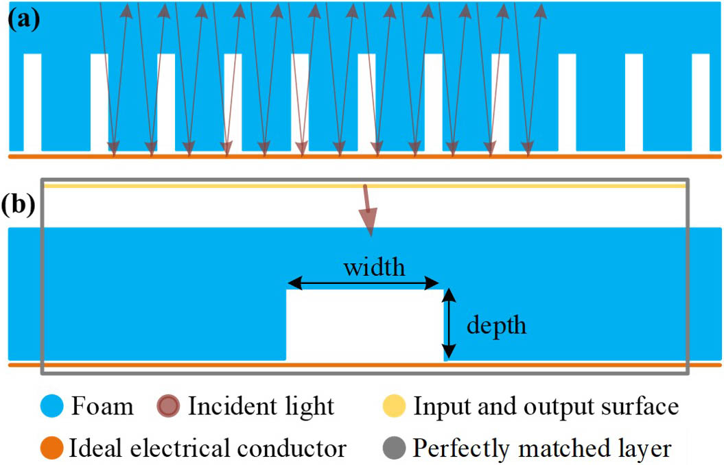
Fig. 2. Defect scattering model. (a) Geometric optical model and (b) electromagnetic scattering model.
Fig. 3. Photograph of the foam board with embedded horizontal strip defects with widths of (a) 0.6 cm and (b) 3 cm; photograph of the (c) defect-free EVA board and (d) blackboard.
Fig. 4. (a) Images of defect-free EVA board at 0.22 THz; (b) comparison of the imaging results and simulations of defect-free EVA.
Fig. 5. 0.22 THz images. 3-cm-width embedded horizontal strip defects with depths of (a1) 0.5 cm, (a2) 1 cm, and (a3) 1.5 cm. 0.6-cm-width embedded horizontal strip defects with depths of (b1) 0.5 cm, (b2) 1 cm, and (b3) 1.5 cm.
Fig. 6. A 3-cm-width defect example. Scattering near-field distributions of partial scanning points of the (a1) defect-free foam board and 3-cm-width strip defect at (b1) yt = 0 cm, (c1) yt = −30 cm and 0.6-cm-width strip defect at (d1) yt = 0 cm, (e1) yt = −30 cm. (a2), (b2), (c2), (d2), and (e2) are the far-field distributions of (a1), (b1), (c1), (d1), and (e1) in front of the MR, respectively.
Fig. 7. Comparison of the 0.22 THz imaging results and the simulations of the defects with depths of (a1), (b1) 0.5 cm, (a2), (b2) 1 cm, and (a3), (b3) 1.5 cm. (a1)–(a3) and (b1)–(b3) are the defects with widths of 0.6 cm and 3 cm, respectively.
Fig. 8. GO simulation results of minimum resolvable distance for two 0.5-cm-width defects. The spacing between the two defects was (a) 3 cm, (b) 2 cm, and (c) 1 cm, respectively.

Set citation alerts for the article
Please enter your email address
© Copyright 2018-2021 | Chinese Laser Press. All Rights Reserved 沪ICP备15018463号-20