
Zhao Chen, Fan Zhang, Qi Zhang, Juanjuan Ren, He Hao, Xueke Duan, Pengfei Zhang, Tiancai Zhang, Ying Gu, Qihuang Gong, "Blue-detuned optical atom trapping in a compact plasmonic structure," Photonics Res. 5, 436 (2017)
- Photonics Research
- Vol. 5, Issue 5, 436 (2017)
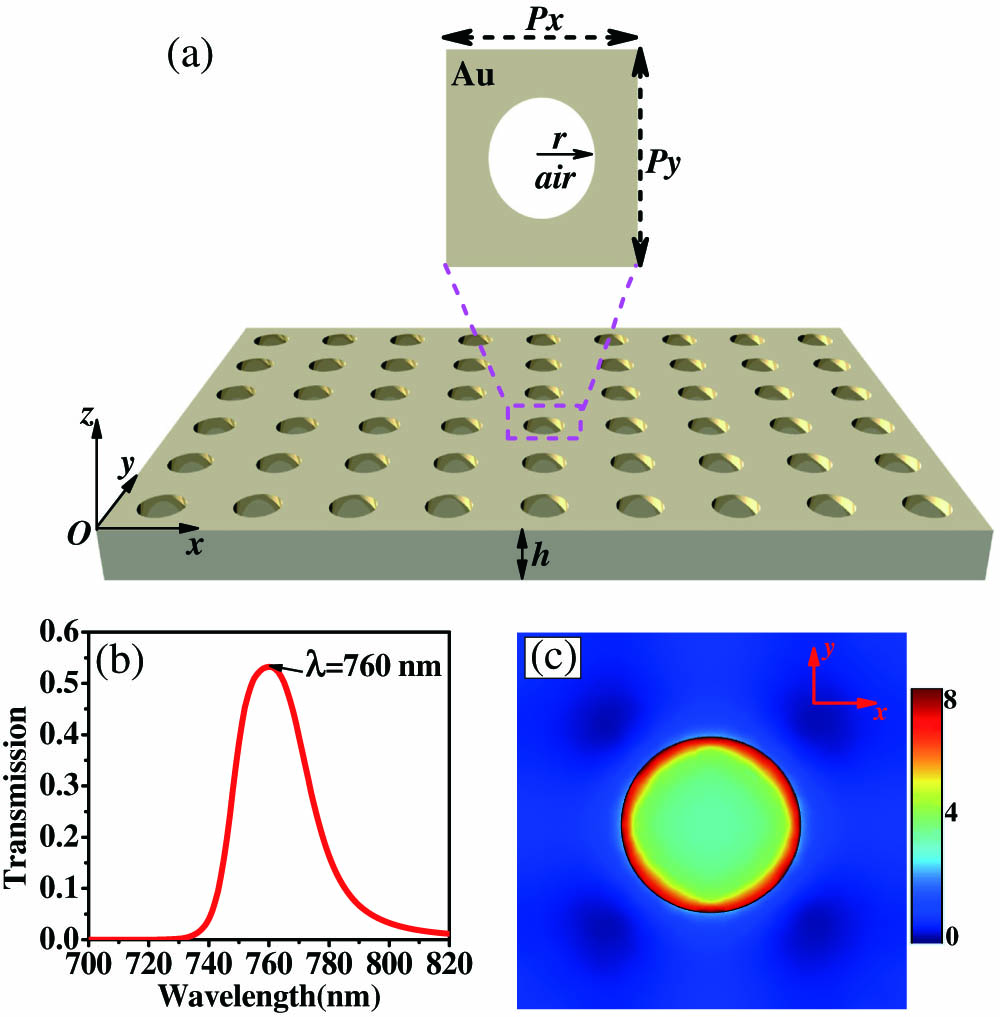
Fig. 1. (a) Schematic of the array of nanoholes in a metallic film. Inset shows the unit cell of the presented nanohole arrays and the geometrical parameter symbols. (b) Simulation results of the normalized zero-order transmission spectrum. (c) Field distribution of | E | − z
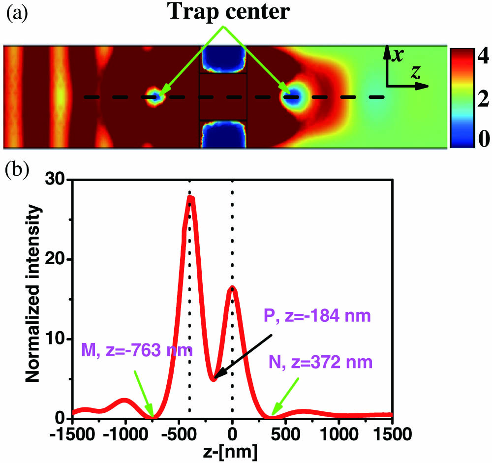
Fig. 2. (a) Field distributions of | E | x – z y | E | 2
Fig. 3. (a) Calculated total potential along the dark dashed line in Fig. 2(a) . (b) Potential distributions for point P x – y U x U tot − x x P 0 = 1 mW
Fig. 4. (a) Contour plot of a trapping total potential in the x – y z = 372 nm


Set citation alerts for the article
Please enter your email address

© Copyright 2018-2021 | Chinese Laser Press. All Rights Reserved 沪ICP备15018463号-20