Abstract
Mode- and polarization-division multiplexing offer new dimensions to increase the transmission capacity of optical communications. Selective switches are key components in reconfigurable optical network nodes. An on-chip silicon 2×2 mode- and polarization-selective switch that can route four data channels on two modes and two polarizations simultaneously is proposed and experimentally demonstrated for the first time, to the best of our knowledge. The overall insertion losses are lower than 8.6 dB. To reduce the inter-modal crosstalk, polarization beam splitters are added to filter the undesired polarizations or modes. The measured inter-modal and intra-modal crosstalk values are below ?23.2 and ?22.8 dB for all the channels, respectively.1. INTRODUCTION
Optical communication technologies have been advancing rapidly for several decades [1–3]. Multiple dimensions of an optical carrier, including time, wavelength, polarization, amplitude, and phase, have been explored to increase data-carrying capacity. Space-division multiplexing (SDM) in multi-core fibers [4,5] and mode-division multiplexing (MDM) in few-mode fibers [6–8] are promising options to increase transmission capacity. Because of the merits of a compact footprint, low power consumption, and compatibility with CMOS fabrication processes [9–12], MDM in silicon photonic integrated circuits has attracted much attention in the past years [13–18].
Switching and routing of data signals are basic requirements in network nodes. In analogy to a conventional wavelength selective switch (WSS) that routes any wavelength channel from one input port to any output port [19], a switch that can route mode- and polarization-multiplexed signals can effectively increase the capacity and add new functionalities. A four-channel silicon switch that used MDM signals on different wavelengths was achieved with crosstalk values of [20]. Recently, we demonstrated an on-chip silicon mode- and polarization-selective switch (MPSS) on the same wavelength with crosstalk values of [21]. These reported crosstalk values need to be reduced to realize error-free switching in practical systems. The power penalty originating from the crosstalk is modulation format dependent [22,23], and typically at least a 20 dB suppression ratio is needed between different modes and polarizations. Moreover, these silicon mode and polarization switches are in configurations, while switches are desired as the fundamental building blocks of a general switch fabric [24].
In this paper, we demonstrate the first on-chip silicon MPSS, to the best of our knowledge. The proposed MPSS can route four data channels of two modes and two polarizations on the same wavelength from one input port to any output port. Polarization beam splitters (PBSs) are added to filter the undesired modes or polarizations; therefore, the measured inter-modal crosstalk values are below at 1550 nm for all the channels. The overall insertion losses and the intra-modal crosstalk values are below 8.6 and , respectively. The footprint of the MPSS device is . The proposed MPSS device needs to couple to few-mode fibers for application in optical fiber communications. Mode converters, such as grating-coupler-based [25] or edge-coupler-based [26,27], are required to couple high-order modes from few-mode fibers to the silicon waveguides.
Sign up for Photonics Research TOC. Get the latest issue of Photonics Research delivered right to you!Sign up now
2. DEVICE DESIGN AND OPERATION PRINCIPLE
The schematic configuration of the on-chip silicon MPSS for two modes and two polarizations is shown in Fig. 1. It can route four channels of , , , and modes. The routing of the channels is realized by the fundamental mode switches. Two transverse electric modes ( and ) and two transverse magnetic modes ( and ) are injected from the input port I1 or I2, and then de-multiplexed into four fundamental mode channels by the mode de-multiplexers and the PBSs based on selective mode coupling in asymmetric directional couplers [12]. Signals are then routed by the corresponding or Mach–Zehnder interferometer (MZI)-based thermal-tuning switches. The routed signals are multiplexed by the polarization beam combiners (PBCs) and the mode multiplexers, and then output from port O1 or O2. The dominant inter-modal crosstalk is induced by the orthogonally polarized modes in the mode multiplexers and de-multiplexers [28]. Therefore, PBSs are cascaded to the mode de-multiplexers to filter the undesired polarizations or modes and reduce the inter-modal crosstalk.
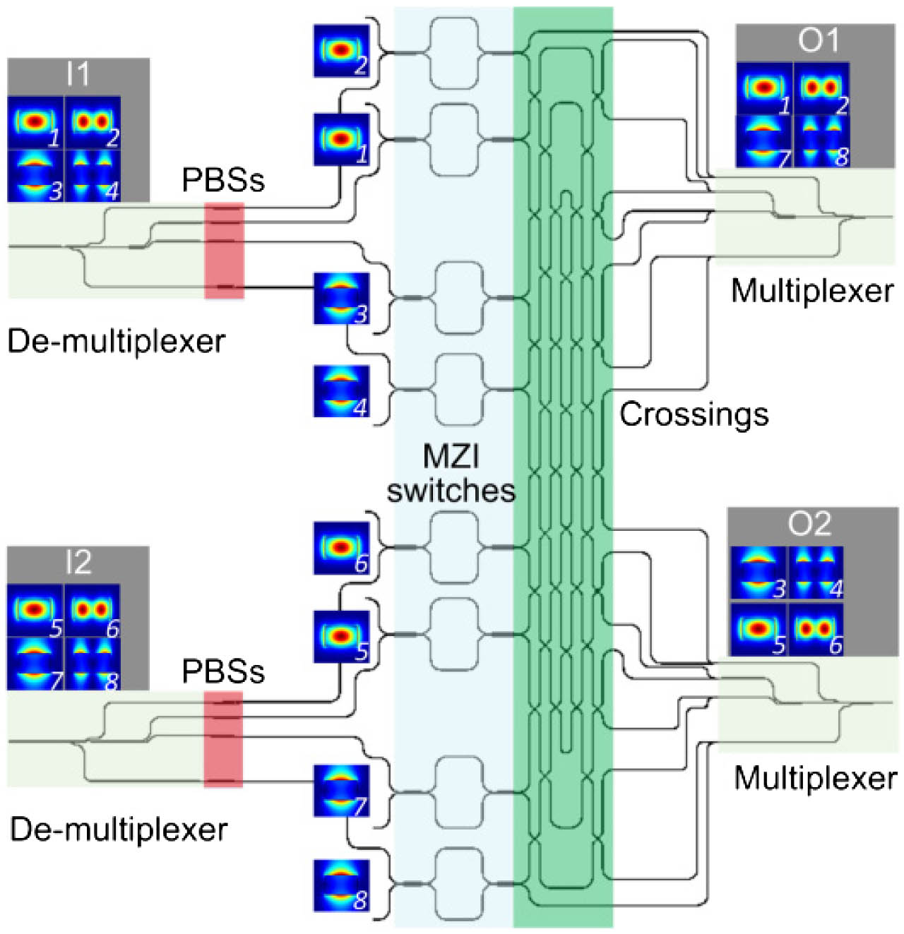
Figure 1.Schematic configuration of the MPSS for two modes and two polarizations. As an example, the and channels of Input 1 and the and channels of Input 2 are routed to Output 1 and other channels are routed to Output 2. The calculated mode patterns of the , , , and modes are intensity profiles. The intensity profiles of the and modes look like second-order TM modes in the normal direction. It is attributed to the small height (220 nm) of the silicon waveguides.
The proposed MPSS chip consists of four mode (de)multiplexers, 10 PBSs, eight thermo-optic MZI switches, eight multi-mode interferometer (MMI) couplers, two PBCs, and 40 waveguide crossings. Figure 2 shows the structures of the basic elements in the MPSS. The PBS (PBC) based on directional couplers [29] is used to separate or combine the and polarizations. The mode (de)multiplexer is implemented by two asymmetric directional couplers to (de)multiplex the high-order modes ( and ) [13], as shown in Fig. 2(a). The widths of the multimode bus waveguide and access waveguides are optimized to achieve highly efficient selective mode coupling by using 3D finite-difference time-domain (FDTD) simulations.

Figure 2.Basic elements of the MPSS. (a) A PBS and a mode multiplexer; (b) a waveguide crossing; (c) a MMI; (d) an MZI switch.
The waveguide widths , , , and are 0.400, 1.035, 0.845, and 1.045 μm, for multiplexing the , , , and modes, respectively. Adiabatic tapers are used to connect the waveguides with different widths. The coupling lengths for multiplexing the , , and modes are 8.25, 18.5, and 8.25 μm, respectively. The maximum number of waveguide crossings in an optical path is seven, so low-loss waveguide crossings are indispensable in the MPSS device. The waveguide crossings are based on 90°-crossed MMIs [30], which are designed to achieve low losses and crosstalk based on 3D-FDTD simulations. The width and length of the MMIs are optimized to be 1.73 μm (1.73 μm) and 7.84 μm (6.14 μm) for the () case, respectively. The MZI switch consists of two MMI couplers connected by two equal-length waveguide arms for broadband operation [31]. For the () polarization, the width and length of the MMI are 6.0 μm (6.0 μm) and 41.5 μm (31.5 μm), respectively, and its input and output waveguides are linearly tapered from 500 nm to 1.4 μm in a length of 8.5 μm to reduce insertion losses. The gap between the two access waveguides is 0.6 μm. The heater lengths in the MZI switches are 50 μm. MMIs are used as 3 dB couplers in the MPSS. The width and length of the MMI are optimized to be 2.4 and 1.8 μm, respectively, and the input and output waveguides of the device are linearly tapered from 500 to 750 nm in a length of 1.5 μm. The gap between the two access waveguides is 0.15 μm.
3. DEVICE FABRICATION AND RESULTS
Multiple MPSS devices were fabricated on a silicon-on-insulator (SOI) wafer (220-nm-thick silicon on 3000-nm-thick silica) by electron-beam lithography (Vistec EBPG 5200) and inductively coupled plasma (ICP) etching. A 1-μm-thick cladding was deposited using plasma enhanced chemical vapor deposition (PECVD). 100-nm-thick Ti heaters and 1-μm-thick Al contact pads were formed by the lift-off process. A microscope photo of a fabricated MPSS chip is shown in Fig. 3(a). Figure 3(b) depicts the magnified scanning electron microscope (SEM) images and microscope photos of a PBS, a mode multiplexer, waveguide crossings, and an MZI switch. The footprint of the MPSS device is less than .
Figure 3.(a) Microscope photo of a fabricated MPSS chip. (b) Magnified SEM images and microscope photos of a PBS, a mode multiplexer, waveguide crossings, and an MZI switch.
In our measurements, grating couplers were used to couple the - and -polarized light into/out of the chip. The design and the measured coupling losses of the grating couplers have been reported previously [32]. The periods of the TE and TM grating couplers are 630 and 1080 nm, respectively. The etching depth of both grating couplers is 70 nm. The coupling losses are and , respectively. To couple the fundamental - and -polarized light into and out of the chip using the grating couplers, mode (de)multiplexers are added to the input (output) ports of the MPSS. The transmission spectra of the MPSS were measured and normalized to that of the identical grating couplers and the mode (de)multiplexers fabricated on the same chip. A tunable continuous wave (CW) laser (Keysight 81960A) and an optical powermeter were used to characterize the devices. For off-chip communications through fibers, mode adapters are needed to couple high-order modes from few-mode fibers to the silicon chip [25,27].
We also fabricated the PBSs, mode (de)multiplexers, and waveguide crossings on the same wafer and characterized the performance of these unit devices. The measured insertion losses of the PBS are 0.54 and 0.83 dB for the and polarizations, respectively. The insertion losses of the mode multiplexer at 1550 nm are 1.60 and 1.32 dB for the and channels, respectively. The measured crosstalk values are lower than at 1550 nm for all the channels. The insertion losses of the fabricated waveguide crossings are lower than 0.09 and 0.12 dB for the TE and TM polarizations, respectively, and the crosstalk values are lower than for both polarizations. The insertion losses and crosstalk values of the building blocks are shown in Table 1.
| Building Block | Insertion Loss (dB) | Crosstalk (dB) |
| PBS for TE0 | 0.54 | −22 |
| PBS for TM0 | 0.83 | −24 |
| Mode multiplexer for TE1 | 1.6 | −18 |
| Mode multiplexer for TM1 | 1.32 | −23 |
| Crossing for TE0 | 0.09 | −35 |
| Crossing for TM0 | 0.12 | −30 |
Table 1. Measured Performance of Building Blocks
The measured transmission spectra of the MPSS device are shown in Fig. 4. Take the channel at input port I1 as an example: the signal is switched to output port O1 when the MZI heating power is 10.45 mW, and the signal is routed to output port O2 when the applied heating power is 25.76 mW. The insertion losses are lower than 5.1 dB at 1550 nm, and are mainly caused by the scattering loss, incomplete coupling in the mode multiplexer and the PBS, and 3 dB coupling loss. For all the other channels, optical signals from different input ports can be routed to arbitrary output ports independently by applying different powers on the corresponding MZI switches. The overall insertion losses are lower than 8.6 dB at 1550 nm for all the channels. The inter-modal crosstalk is a critical challenge toward realizing error-free switching in practical systems. We measured the inter-modal crosstalk between channels by launching a signal to a fixed input port and measuring the transmission responses at each output port one by one, as shown in Fig. 4. The MZI switches were set to ensure the maximum output powers at the same output port. For example, when a signal was injected to the channel and the response was measured at the channel, the MZI switches for the and channels were both set to output to the O2 port. The measured inter-modal crosstalk values are lower than for all the channels at 1550 nm. The power consumption of a TM MZI thermo-optic switch is higher than that of a TE switch due to the smaller optical confinement factor of the TM mode in a silicon waveguide. The measured switching powers for the TM channels are higher than that for the TE channels, except that for the channel. We attribute the channel results to fabrication imperfections.
Figure 4.Measured inter-modal crosstalk performance.
We further measured the intra-modal crosstalk values introduced by the MZI switches, as shown in Fig. 5. For the channel of port I1, the intra-modal crosstalk values are lower than at 1550 nm. For all the channels, the overall intra-modal crosstalk values are below at 1550 nm. The different wavelength dependency among modes is attributed to different coupling lengths and waveguide widths of the asymmetric directional couplers. Some noise is attributed to imperfections introduced in the fabrication and the low received power, which is close to the detection limit of the optical powermeter.
Figure 5.Measured intra-modal crosstalk performance.
These inter- and intra-modal crosstalk values are comparable to those of integrated mode-multiplexer devices [13,15,33], indicating that the MPSS exhibits low crosstalk. The switching capacity of the MPSS can be further scaled when combining with wavelength-division multiplexing technology, while maintaining the same switching granularity [21]. Mode- and polarization-multiplexed signals are first demultiplexed to enable single-mode operation for the subsequent wavelength de-multiplexing. Such a new mode-, polarization-, and wavelength-selective switch (MPWSS) may become an important building block in future high-capacity optical networks.
The switching time of the MPSS device was measured by applying a square electric wave to one heater and detecting the output power simultaneously by a photodetector. The rise time and fall time are 5.5 and 4.9 μs, respectively. In the experiment, we tried to find the switching power to obtain the maximum output optical power manually, while it is possible to achieve switch control and calibration with built-in power monitors and a feedback loop [34,35].
4. CONCLUSION
We propose and experimentally demonstrate what we believe is the first on-chip silicon MPSS, which is the fundamental building block of an switch matrix. To reduce the inter-modal crosstalk values, PBSs are added to filter the undesired polarizations or modes. The measured inter-modal crosstalk values are below at 1550 nm. For all the channels, the overall insertion losses are . The measured intra-modal crosstalk values introduced by the MZI switches are lower than .
Acknowledgment
Acknowledgment. We thank the Center for Advanced Electronic Materials and Devices (AEMD) of Shanghai Jiao Tong University for the support in device fabrication.
References
[1] P. J. Winzer. Making spatial multiplexing a reality. Nat. Photonics, 8, 345-348(2014).
[2] H.-L. Zhou, D.-Z. Fu, J.-J. Dong, P. Zhang, D.-X. Chen, X.-L. Cai, F.-L. Li, X.-L. Zhang. Orbital angular momentum complex spectrum analyzer for vortex light based on the rotational Doppler effect. Light Sci. Appl., 6e, e16251(2017).
[3] Y. Kodama, Y. Yamaguchi, A. Kanno, T. Kawanishi, M. Izutsu, H. Nakajima. Mode-division multiplexing LiNbO3 modulator using directional coupler. OptoElectronics and Communications Conference (OECC) held jointly with International Conference on Photonics in Switching (PS), ThD3-5(2016).
[4] D. Richardson, J. Fini, L. Nelson. Space-division multiplexing in optical fibres. Nat. Photonics, 7, 354-362(2013).
[5] Y. Ding, V. Kamchevska, K. Dalgaard, F. Ye, R. Asif, S. Gross, M. J. Withford, M. Galili, T. Morioka, L. K. Oxenløwe. Reconfigurable SDM switching using novel silicon photonic integrated circuit. Sci. Rep., 6, 39058(2016).
[6] R. Ryf, S. Randel, N. K. Fontaine, M. Montoliu, E. Burrows, S. Chandrasekhar, A. H. Gnauck, C. Xie, R.-J. Essiambre, P. Winzer, R. Delbue, P. Pupalaikis, A. Sureka, Y. Sun, L. Gruner-Nielsen, R. V. Jensen, R. Lingle. 32-bit/s/Hz spectral efficiency WDM transmission over 177-km few-mode fiber. Optical Fiber Communication Conference/National Fiber Optic Engineers Conference, PDP5A.1(2013).
[7] N. Bai, E. Ip, Y.-K. Huang, E. Mateo, F. Yaman, M.-J. Li, S. Bickham, S. Ten, J. Liñares, C. Montero, V. Moreno, X. Prieto, V. Tse, K. Man Chung, A. P. T. Lau, H.-Y. Tam, C. Lu, Y. Luo, G.-D. Peng, G. Li, T. Wang. Mode-division multiplexed transmission with inline few-mode fiber amplifier. Opt. Express, 20, 2668-2680(2012).
[8] J. Zhao, M. Tang, K. Oh, Z. Feng, C. Zhao, R. Liao, S. Fu, P. P. Shum, D. Liu. Polarization-maintaining few mode fiber composed of a central circular-hole and an elliptical-ring core. Photon. Res., 5, 261-266(2017).
[9] D. Dai, J. Bauters, J. E. Bowers. Passive technologies for future large-scale photonic integrated circuits on silicon: polarization handling, light non-reciprocity and loss reduction. Light Sci. Appl., 1, e1(2012).
[10] Z. Zhou, B. Yin, Q. Deng, X. Li, J. Cui. Lowering the energy consumption in silicon photonic devices and systems. Photon. Res., 3, B28-B46(2015).
[11] L. Thylén, L. Wosinski. Integrated photonics in the 21st century. Photon. Res., 2, 75-81(2014).
[12] Y. Zhang, Y. He, J. Wu, X. Jiang, R. Liu, C. Qiu, X. Jiang, J. Yang, C. Tremblay, Y. Su. High-extinction-ratio silicon polarization beam splitter with tolerance to waveguide width and coupling length variations. Opt. Express, 24, 6586-6593(2016).
[13] D. Dai, J. Wang, Y. Shi. Silicon mode (de)multiplexer enabling high capacity photonic networks-on-chip with a single-wavelength-carrier light. Opt. Lett., 38, 1422-1424(2013).
[14] L.-W. Luo, N. Ophir, C. P. Chen, L. H. Gabrielli, C. B. Poitras, K. Bergmen, M. Lipson. WDM-compatible mode-division multiplexing on a silicon chip. Nat. Commun., 5, 3069(2014).
[15] J. Wang, S. He, D. Dai. On-chip silicon 8-channel hybrid (de)multiplexer enabling simultaneous mode- and polarization-division-multiplexing. Laser Photon. Rev., 8, L18-L22(2014).
[16] D. Dai, J. Wang, S. Chen, S. Wang, S. He. Monolithically integrated 64-channel silicon hybrid demultiplexer enabling simultaneous wavelength- and mode-division-multiplexing. Laser Photon. Rev., 9, 339-344(2015).
[17] X. Wu, K. Xu, D. Dai, H. Tsang. Mode division multiplexing switch for on-chip optical interconnects. OptoElectronics and Communications Conference (OECC) held jointly with International Conference on Photonics in Switching (PS), ThE2-4(2016).
[18] D. Dai, S. Wang. Silicon-based reconfigurable optical add-drop multiplexer for hybrid MDM-WDM systems. Optical Fiber Communication Conference, Tu2C.1(2017).
[19] C. R. Doerr, L. L. Buhl, L. Chen, N. Dupuis. Monolithic flexible-grid 1× 2 wavelength-selective switch in silicon photonics. J. Lightwave Technol., 30, 473-478(2012).
[20] B. Stern, X. Zhu, C. P. Chen, L. D. Tzuang, J. Cardenas, K. Bergman, M. Lipson. On-chip mode-division multiplexing switch. Optica, 2, 530-535(2015).
[21] Y. Zhang, Q. Zhu, Y. He, C. Qiu, Y. Su, R. Soref. Silicon 1 × 2 mode- and polarization-selective switch. Optical Fiber Communication Conference, W4E.2(2017).
[22] P. Winzer, A. Gnauck, A. Konczykowska, F. Jorge, J.-Y. Dupuy. Penalties from in-band crosstalk for advanced optical modulation formats. 37th European Conference and Exposition on Optical Communications, Tu.5.B.7(2011).
[23] Y. Ding, J. Xu, F. Da Ros, B. Huang, H. Ou, C. Peucheret. On-chip two-mode division multiplexing using tapered directional coupler-based mode multiplexer and demultiplexer. Opt. Express, 21, 10376-10382(2013).
[24] A. W. Poon, X. Luo, F. Xu, H. Chen. Cascaded microresonator-based matrix switch for silicon on-chip optical interconnection. Proc. IEEE, 97, 1216-1238(2009).
[25] B. Wohlfeil, C. Stamatiadis, L. Zimmermann, K. Petermann. Compact fiber grating coupler on SOI for coupling of higher order fiber modes. Optical Fiber Communication Conference and Exposition and the National Fiber Optic Engineers Conference (OFC/NFOEC), OTh1B.2(2013).
[26] D. Melati, A. Alippi, A. Melloni. Reconfigurable photonic integrated mode (de)multiplexer for SDM fiber transmission. Opt. Express, 24, 12625-12634(2016).
[27] D. Dai, M. Mao. Mode converter based on an inverse taper for multimode silicon nanophotonic integrated circuits. Opt. Express, 23, 28376-28388(2015).
[28] J. Wang, P. Chen, S. Chen, Y. Shi, D. Dai. Improved 8-channel silicon mode demultiplexer with grating polarizers. Opt. Express, 22, 12799-12807(2014).
[29] D. Dai. Silicon polarization beam splitter based on an asymmetrical evanescent coupling system with three optical waveguides. J. Lightwave Technol., 30, 3281-3287(2012).
[30] Y. Liu, J. M. Shainline, X. Zeng, M. A. Popović. Ultra-low-loss CMOS-compatible waveguide crossing arrays based on multimode Bloch waves and imaginary coupling. Opt. Lett., 39, 335-338(2014).
[31] T. Chu, H. Yamada, S. Ishida, Y. Arakawa. Compact 1 × N thermo-optic switches based on silicon photonic wire waveguides. Opt. Express, 13, 10109-10114(2005).
[32] Y. Zhang, Y. He, X. Jiang, B. Liu, C. Qiu, Y. Su, R. A. Soref. Ultra-compact and highly efficient silicon polarization splitter and rotator. APL Photon., 1, 091304(2016).
[33] J. B. Driscoll, C. P. Chen, R. R. Grote, B. Souhan, J. I. Dadap, A. Stein, M. Lu, K. Bergman, R. M. Osgood. A 60 Gb/s MDM-WDM Si photonic link with <0.7 dB power penalty per channel. Opt. Express, 22, 18543-18555(2014).
[34] X. Zheng, E. Chang, P. Amberg, I. Shubin, J. Lexau, F. Liu, H. Thacker, S. S. Djordjevic, S. Lin, Y. Luo, J. Yao, J.-H. Lee, K. Raj, R. Ho, J. E. Cunningham, A. V. Krishnamoorthy. A high-speed, tunable silicon photonic ring modulator integrated with ultra-efficient active wavelength control. Opt. Express, 22, 12628-12633(2014).
[35] H. Jayatilleka, K. Murray, M. Á. Guillén-Torres, M. Caverley, R. Hu, N. A. F. Jaeger, L. Chrostowski, S. Shekhar. Wavelength tuning and stabilization of microring-based filters using silicon in-resonator photoconductive heaters. Opt. Express, 23, 25084-25097(2015).

