
Yirong Su, Wenbo Ma, Yang (Michael) Yang. Perovskite semiconductors for direct X-ray detection and imaging[J]. Journal of Semiconductors, 2020, 41(5): 051204
- Journal of Semiconductors
- Vol. 41, Issue 5, 051204 (2020)
Abstract
1. Introduction
X-ray possesses strong penetrating capacity, so has been widely applied to nondestructively probe the inside information of condensed matter subjects in various fields, e.g., industrial inspection, security check, medical examination, scientific research and so on[
Nowadays, two approaches are used to detect X-ray[
During the last decade, halide perovskites have emerged as a new generation of photoelectric materials and its remarkable performance has been attractive in the fields of solar cells, light-emitting diodes, lasers, photodetectors, etc.[
This review will introduce the fundamental principle of direct X-ray detection and imaging, summarize the advances of perovskite materials for this purpose and finally put forward some needful and feasible directions in this field.
2. Mechanism of X-ray interacting with matter
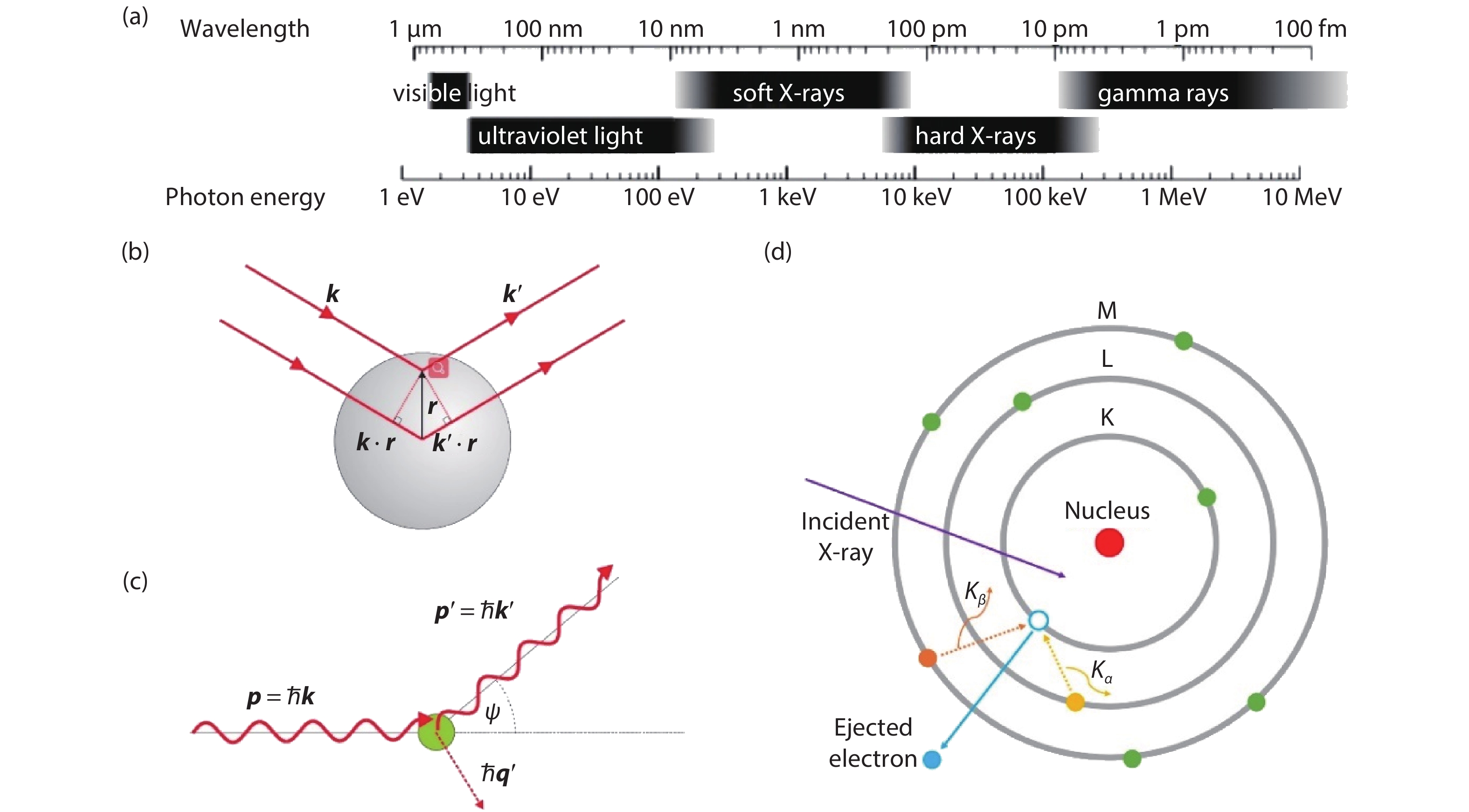
X-rays are electromagnetic waves with wavelengths ranging from 0.01 to 10 nm (Fig. 1(a)). From a quantum mechanical perspective, a beam of X-rays can be quantized into photons of which the photon energy is tens of thousands of times greater than that of visible light. The intensity of X-rays is then given by the number of photons passing through a given area per unit time. There are two ways of interaction between X-ray photon and matter: scattering and absorption.
![]()
Figure 1.(Color online) (a) Spectrum region of X-ray to wavelength and photon energy. (b) Thomson scattering from an atom. An X-ray with a wave vector
2.1. Scattering of X-ray
X-ray scattering can be divided into two types: Thomson scattering and Compton scattering. As shown in Fig. 1(b), Thomson scattering is elastic scattering of X-ray radiation by a free charged particle, which won’t change the kinetic energy and frequency of X-ray photon. Thomson scattering is also coherent and its coherence makes it exploited in investigations of the structure of materials. when Bragg’s law is fulfilled, the X-ray will be elastic scattered from a crystal and coherently add up, then the scattering is restricted to lie at points on the reciprocal lattice. On the contrary, Compton scattering (Fig. 1(c)) is inelastic and incoherent scattering where the energy of incident X-ray photon may be transferred to the electron, resulting in lower frequency of scattered photon relative to that of incident one. The unique information on the electronic structure of materials could be obtained by Compton scattering. As the energy of incident X-ray photon is increased, the scattering becomes progressively more inelastic for a given scattering angle[
2.2. Photoelectric absorption of X-ray
Fig. 1(d) illustrates the process of photoelectric absorption. After the incident X-ray photon is absorbed by an atom, the excess energy is transferred to an electron which will be ejected from the inner atom shell, creating a hole in that shell and leaving the atom ionized. The hole is subsequently filled by an electron from an outer shell with the simultaneous emission of a characteristic X-ray photon, of which the energy equals to the difference in the binding energies of electrons in these two shells. The characteristic emission X-ray is often used in X-ray fluorescence (XRF) analysis. By the way, the ionized atom could fill the hole in inner shell by expelling Auger electron as well.
The X-ray absorption can be quantitatively calculated by the following formula[
where the I0 and I(d) are the X-ray intensities when the thicknesses are zero and d, μ is the linear absorption coefficient, d is the thickness, σ is the X-ray absorption cross-section and ρ is the density of matter. The absorption cross-section σ is a function of X-ray photon energy (
It could be concluded that high energy X-ray has strong penetrating capability and the matter with heavy atoms is able to attenuate X-ray more efficiently. It is how the X-ray imaging is realized, and X-ray detection also puts forward some requirements to the detection materials for the same reason.
3. Direct X-ray detection and perovskite X-ray detectors
Direct detection is realized utilizing the ionization capacity of X-ray. When X-ray reaches a direct detector, the detecting materials are ionized, generating many free charges by the photoelectric effect and Compton scattering. In these two processes, the energy of X-ray photons is directly transferred to lots of charges, and then these excess charges are collected by electrodes under certain bias.
3.1. Ion chamber
The gas-filled detector worked at the voltage of ionization region (100 to 200 V), which is known as ion chamber[
![]()
Figure 2.(Color online) (a) Working Principle of ion chamber. Reproduced with permission from Ref. [
3.2. Semiconductor X-ray detectors
3.2.1. Mechanism of semiconductor detectors
Direct X-ray semiconductor detector have become an attractive research field in recent years due to its good absorption, high sensitivity, fast response and excellent energy resolution[
3.2.2. Parameters of semiconductor detectors
The direct X-ray detection is generally considered to consist of three processes: absorption of X-ray energy, generation of carries (EHPs) and transport of charges[
In the first process, the atomic number (Z) and density (ρ) of the detection material determine the linear absorption coefficient (μ), which represents the X-ray stopping power of this material at per unit thickness under certain photon energy. Fig 2(c) shows the linear absorption coefficients of different kinds of perovskites and some conventional X-ray detecting materials. In order to maximize X-ray energy utilization and reduce the risk of radiation leakage, semiconductor layer needs sufficient thickness to completely absorb X-rays. However, larger thickness tends to cause undesirable problems. For example, it is difficult to fabricate large area thick film with high quality and the thick semiconductor has lower charge collection efficiency in most cases. Besides, a larger thickness can also damage the imaging quality of X-ray, because the lateral charge transport will cause signal crosstalk in the image read out circuit[
In the carriers generation process, the EHP creation energy (W±), which is defined as the amount of radiation energy required to create a single EHP, should be as small as possible because the free charge (ΔQ) generated from an absorbed radiation of energy (ΔE) could be calculated by the following formula[
where e is the elementary charge. W± is proportional to the bandgap (Eg) in many material systems. It is well-known that W± ≈ 3Eg for many crystalline semiconductors, which is so-called Klein rule[
The transport and collection of carries is a pretty complicated process in semiconductor X-ray detector, and various of parameters are related. The central parameter is the product of carrier mobility and mean carrier lifetime (μτ), which is normally called the range of the carrier. It represents the mean distance drifted by the carrier per unit electric field before the carrier disappears by recombination (or trapped by defects)[
3.2.3. Development status of semiconductor X-ray detectors
Since Van Heerden first investigated silver chloride (AgCl) crystals as radiation detectors in 1945[
3.2.4. Advantages of perovskite for semiconductor X-ray detectors
In recent years, halide perovskites (composition of ABX3, X = Cl, Br or I) have revolutionized the development of compound semiconductor X-ray detectors due to many beneficial qualities of them. Firstly, each of common elements in halide perovskite material systems, e.g., Cs, Pb, Bi, Br and I, has a high Z, meaning a strong stopping power and a favorable absorption efficiency. Meanwhile, narrower bandgaps of halide perovskites give rise to smaller W±, which produce high intrinsic X-ray sensitivity. Furthermore, perovskites own outstanding charge transportation ability (long carrier lifetime and low trap density), leading to their μτ products much better than that of conventional compound semiconductor X-ray detectors[
In addition to their superior performances, solution-processed perovskites have another significant advantage, i.e. the low cost both in raw materials and manufacturing techniques[
3.3. Development progress of perovskite X-ray detectors
3.3.1. Advance in perovskite single crystal X-ray detectors
Single crystal is quite infrequent in the past compound semiconductor X-ray detectors, because the single crystal growth process of other materials is often expensive and hard to obtain a bulk of big enough single crystal for flat panel imaging. But now in perovskites, this situation has been changed. Dong et al. have successfully fabricated organolead trihalide perovskite (OTP) single crystal (MAPbI3, MA = CH3NH3) with long carrier diffusion lengths (> 175μm) by low-cost solution-grown method in 2015[
Compared with MAPbBr3 single crystal, X-ray detector made by MAPbI3 single crystal is rather limited although its X-ray stopping power is stronger. Ye et al. thought it was probably because the natural geometry of MAPbI3 single crystals is usually nonrectangular dodecahedrons, which is not as feasible as cuboid-shaped single crystals (such as MAPbBr3) for device fabrications, especially for flat-panel array[
Because Pb2+ can severely damage the human brain and threaten the biological systems for the high solubility in water, the toxicity of lead halide perovskites should not be neglected[
In addition to double perovskites, another low-dimensional and bismuth halide perovskite materials system has also received attention due to its unique anisotropic performance. Zhuang et al. showed their 2D layered perovskite-like (NH4)3Bi2I9 X-ray detector revealing high sensitivity of 8.2 × 10³μC/(Gy·cm2) in the parallel direction and low detection limit of 55 nGy/s in the perpendicular direction[
Fig. 2(e) shows some graphs of single crystals among part of representative perovskites discussed above, and Fig. 2(f) schematically illustrates the method of inverse temperature crystallization (ITC), which is a common and low-cost method for synthesis of perovskite single crystals[
3.3.2. Large-area fabrication of polycrystalline perovskites for X-ray detection
Actually, the first time of polycrystalline perovskites X-ray detection was before that of single crystal detection. Even so the material systems of polycrystalline perovskites X-ray detection have been hardly innovated, while the fabrication technique of large-area polycrystalline perovskite thick films for X-ray imaging has made great progress. Yakunin et al. firstly tried to detect X-ray and carry out X-ray imaging using a piece of polycrystalline perovskite solar cell (Fig. 2(g))[
In addition, two crafts have been presented for potential fabrication of large-area and high-quality polycrystalline perovskite thick films applied in X-ray imaging. The first one is a mechanical sintering process to fabricate polycrystalline MAPbI3 wafers with millimeter-scale thickness and well-defined crystallinity (Fig. 2(i))[
4. X-ray imaging based on perovskite detectors
4.1. Evaluation indicators of X-ray imaging
Spatial resolution is a vital performance of an X-ray imaging system. While the spatial resolution of imaging system promoted, the clearer X-ray images would be collected. The spatial resolution of the imaging system can be determined with the modulation transfer function (MTF), representing the transfer ability of input signal modulation of the spatial frequency (in line pair per millimeter; lp/mm or cycles per millimeter; cy/ mm) relative to its output[
The slanted-edge method is frequently used to measure the curve of MTF[
![]()
Figure 3.(Color online) (a) X-ray image of resolution test chart. Reproduced with permission from Ref. [
where x is the position of pixel and f is the spatial frequency. Another approach to determine MTF is very visualized, which is to take X-ray image for an X-ray resolution test chart. As shown in Fig. 3(b), this test chart made by lead film consists of many line pairs with different intervals, representing a series of spatial frequencies from low to high. The MTF of X-ray system can be estimated by observing the definition at each spatial frequency.
4.2. Common X-ray imaging systems using direct detection scenario
The most common X-ray imaging system by direct detection is flat panel X-ray imager (FPXI)[
The spatial resolution of direct FPXI is usually much higher than that of indirect X-ray imaging system because the X-ray is not scattered but scintillation is strongly scattered in scintillators. The theoretical limit of the MTF for an FPXI is a two-dimensional sinc function in diagonal direction dominated by the pixel aperture (a)[
where f is the spatial frequency. Based on the idealized situation, several factors are influencing the MTF of direct FPXI. The design of FPXI generally allows only one type of carriers (electron or hole) to be collected by TFTs[
In current commercial direct FPXIs, the material of choice is stabilized amorphous selenium (a-Se)[
![]()
Figure 4.(Color online) (a) Left: Anrad’s mammographic FPXI (AXS-2430) is used in mammography markets. The field of view is 24 × 30 cm2 and the FPXI have a pixel pitch of 85
4.3. Advances of X-ray imaging based on perovskite direct-type detectors
As described above in Section 3.3, direct X-ray imaging demonstrations based on perovskite have been achieved by various means. Yakunin et al. used a MAPbI3 based solar cell as a single-pixel X-ray detector, carried out scanning of the object and demonstrated a simple X-ray image of piece of leaf (Fig. 4(b))[
Kim et al. referred the design philosophy of a-Se FPXIs, firstly manufactured a true sense of perovskite-based FPXI and successfully realized large-area X-ray imaging[
In addition, Yang et al. fabricated a large-area (5 cm of diameter) Cs2AgBiBr6 polycrystalline wafer by the isostatic-pressing process, then Au electrodes array was thermally evaporated on the wafer to accomplish preliminary X-ray imaging (6 × 6 array, Fig. 4(d))[
On the other hand, X-ray imaging attempts by means of perovskite single crystals have made some good advances as well. Wei et al. reported a low-temperature solution-processed molecular bonding method with the assistance of brominated APTES molecules[
5. Summary and outlook
From this review, it could be seen that direct-type perovskite X-ray detection and imaging have revealed vast potentials for future applications. Compared to a-Se, perovskite semiconductor has many significant advantages including strong X-ray stopping power, remarkable carrier transport ability, high intrinsic sensitivity, low detection limit and inexpensive solution-processed fabrication. However, there still exist some issues to be addressed to facilitate the commercialization.
Firstly, more physical insights are encouraged to understand and guide the material optimization and device design in order to fulfill high sensitivity and low noise. For example, the narrower bandgap leads to smaller W±, and higher intrinsic X-ray sensitivity, while the broader bandgap material usually gives larger resistance and therefore lower noise. Hence, an optimal bandgap needs to be selected for the sake of balancing sensitivity and noise, after all, the X-ray imaging requires adequate SNR with as low dose as possible. We might overemphasized on high sensitivity while ignored the noise reduction, particularly those devices with large trap-assisted photoconductive gains, they might not be so useful for practical applications, because the noises are also increased because of the traps, and ultimately the SNRs are sacrificed. Secondly, it is important to understand and identify the factors that limit the special resolution of the X-ray imaging. It was found that perovskite-based FPXI had much lower spatial resolution than that of a-Se[
In conclusion, more efforts should be contributed to the theorical understanding, fabrication methods and attempting of new materials for perovskite direct X-ray detectors. We believe that the perovskites will emerge as a splendid X-ray detecting material and hold a bright future for practical X-ray imaging applications.
References
[1] M Spahn. X-ray detectors in medical imaging. Nucl Instrum Methods Phys Res A, 731, 57(2013).
[2] C W Van Eijk. Inorganic scintillators in medical imaging. Phys Med Biol, 47, R85(2002).
[3] X Duan, J Cheng, L Zhang et al. X-ray cargo container inspection system with few-view projection imaging. Nucl Instrum Methods Phys Res A, 598, 439(2009).
[4] R P Haff, N Toyofuku. X-ray detection of defects and contaminants in the food industry. Sens Instrum Food Quality Safety, 2, 262(2008).
[5] H N Chapman, P Fromme, A Barty et al. Femtosecond X-ray protein nanocrystallography. Nature, 470, 73(2011).
[6] J A Nielsen, D McMorrow. Elements of modern X-ray physics. Wiley(2011).
[7] W W Moses. Scintillator requirements for medical imaging. LBNL Publications(1999).
[8]
[9] G F Knoll. Radiation detection and measurement. John Wiley & Sons(2010).
[10] J A Rowlands. Medical imaging: Material change for X-ray detectors. Nature, 550, 47(2017).
[11] S Kasap, J B Frey, G Belev et al. Amorphous and polycrystalline photoconductors for direct conversion flat panel X-ray image sensors. Sensors, 11, 5112(2011).
[12] X Zheng, B Chen, J Dai et al. Defect passivation in hybrid perovskite solar cells using quaternary ammonium halide anions and cations. Nat Energy, 2, 17102(2017).
[13] Z Xiao, R A Kerner, L Zhao et al. Efficient perovskite light-emitting diodes featuring nanometre-sized crystallites. Nat Photonics, 11, 108(2017).
[14] M Saliba, S M Wood, J B Patel et al. Structured organic–inorganic perovskite toward a distributed feedback laser. Adv Mater, 28, 923(2016).
[15] L Dou, Y M Yang, J You et al. Solution-processed hybrid perovskite photodetectors with high detectivity. Nat Commun, 5, 5404(2014).
[16] H Wei, Y Fang, P Mulligan et al. Sensitive X-ray detectors made of methylammonium lead tribromide perovskite single crystals. Nat Photonics, 10, 333(2016).
[17] W Pan, H Wu, J Luo et al. Cs2AgBiBr6 single-crystal X-ray detectors with a low detection limit. Nat Photonics, 11, 726(2017).
[18] R Zhuang, X Wang, W Ma et al. Highly sensitive X-ray detector made of layered perovskite-like (NH4)3Bi2I9 single crystal with anisotropic response. Nat Photonics, 13, 602(2019).
[19] W Wei, Y Zhang, Q Xu et al. Monolithic integration of hybrid perovskite single crystals with heterogenous substrate for highly sensitive X-ray imaging. Nat Photonics, 11, 315(2017).
[20] S Yakunin, M Sytnyk, D Kriegner et al. Detection of X-ray photons by solution-processed lead halide perovskites. Nat Photonics, 9, 444(2015).
[21] Y C Kim, K H Kim, D Y Son et al. Printable organometallic perovskite enables large-area, low-dose X-ray imaging. Nature, 550, 87(2017).
[22] J E Martin. Physics for radiation protection: a handbook. John Wiley & Sons(2006).
[23] H Wei, J Huang. Halide lead perovskites for ionizing radiation detection. Nat Commun, 10, 1066(2019).
[24] R Devanathan, L R Corrales, F Gao et al. Signal variance in gamma-ray detectors—A review. Nucl Instrum Methods Phys Res A, 565, 637(2006).
[25] M Kabir. Effects of charge carrier trapping on polycrystalline PbO X-ray imaging detectors. J Appl Phys, 104, 074506(2008).
[26] C A Klein. Bandgap dependence and related features of radiation ionization energies in semiconductors. J Appl Phys, 39, 2029(1968).
[27] R Alig, S Bloom. Electron-hole-pair creation energies in semiconductors. Phys Rev Lett, 35, 1522(1975).
[28]
[29] K G McKay. A. germanium counter. Phys Rev, 76, 1537(1949).
[30] M Guerra, M Manso, S Longelin et al. Performance of three different Si X-ray detectors for portable XRF spectrometers in cultural heritage applications. J Instrum, 7, C10004(2012).
[31] A Owens, A Peacock. Compound semiconductor radiation detectors. Nucl Instrum Methods Phys Res A, 531, 18(2004).
[32] S Del Sordo, L Abbene, E Caroli et al. Progress in the development of CdTe and CdZnTe semiconductor radiation detectors for astrophysical and medical applications. Sensors, 9, 3491(2009).
[33] P Luke, C Rossington, M Wesela. Low energy X-ray response of Ge detectors with amorphous Ge entrance contacts. IEEE Trans Nucl Sci, 41, 1074(1994).
[34] C Szeles. CdZnTe and CdTe materials for X-ray and gamma ray radiation detector applications. Phys Status Solidi B, 241, 783(2004).
[35] G Zentai, M Schieber, L Partain et al. Large area mercuric iodide and lead iodide X-ray detectors for medical and non-destructive industrial imaging. J Cryst Growth, 275, e1327(2005).
[36]
[37] R Street, S Ready, K Van Schuylenbergh et al. Comparison of PbI2 and HgI2 for direct detection active matrix X-ray image sensors. J Appl Phys, 91, 3345(2002).
[38] M Schieber, H Hermon, A Zuck et al. Thick films of X-ray polycrystalline mercuric iodide detectors. J Cryst Growth, 225, 118(2001).
[39] G Zentai, L D Partain, R Pavlyuchkova et al. Mercuric iodide and lead iodide X-ray detectors for radiographic and fluoroscopic medical imaging In: Medical Imaging 2003: Physics of Medical Imaging. International Society for Optics and Photonics, 77(2003).
[40] M S Yun, S H Cho, R Lee et al. Investigation of PbI2 film fabricated by a new sedimentation method as an X-ray conversion material. Jpn J Appl Phys, 49, 041801(2010).
[41] K Shah, R Street, Y Dmitriyev et al. X-ray imaging with PbI2-based a-Si: H flat panel detectors. Nucl Instrum Methods Phys Res A, 458, 140(2001).
[42] M Simon, R Ford, A Franklin et al. Analysis of lead oxide (PbO) layers for direct conversion X-ray detection. IEEE Symposium Conference Record Nuclear Science, 4268(2004).
[43] N Destefano, M Mulato. Influence of multi-depositions on the final properties of thermally evaporated TlBr films. Nucl Instrum Methods Phys Res A, 624, 114(2010).
[44] K Hitomi, Y Kikuchi, T Shoji et al. Improvement of energy resolutions in TlBr detectors. Nucl Instrum Methods Phys Res A, 607, 112(2009).
[45] T M Brenner, D A Egger, L Kronik et al. Hybrid organic–inorganic perovskites: low-cost semiconductors with intriguing charge-transport properties. Nat Rev Mater, 1, 15007(2016).
[46] F P G de Arquer, A Armin, P Meredith et al. Solution-processed semiconductors for next-generation photodetectors. Nat Rev Mater, 2, 16100(2017).
[47] S Kasap. Low-cost X-ray detectors. Nat Photonics, 9, 420(2015).
[48] F Lang, N H Nickel, J Bundesmann et al. Radiation hardness and self-healing of perovskite solar cells. Adv Mater, 28, 8726(2016).
[49] S Yang, Z Xu, S Xue et al. Organohalide lead perovskites: more stable than glass under gamma-ray radiation. Adv Mater, 31, 1805547(2019).
[50] J Huang, Y Yuan, Y Shao et al. Understanding the physical properties of hybrid perovskites for photovoltaic applications. Nat Rev Mater, 2, 17042(2017).
[51] F Lang, O Shargaieva, V V Brus et al. Influence of radiation on the properties and the stability of hybrid perovskites. Adv Mater, 30, 1702905(2018).
[52] Q Dong, Y Fang, Y Shao et al. Electron–hole diffusion lengths > 175
[53] F Ye, H Lin, H Wu et al. High-quality cuboid CH3NH3PbI3 single crystals for high performance X-ray and photon detectors. Adv Funct Mater, 29, 1806984(2019).
[54] M I Saidaminov, A L Abdelhady, B Murali et al. High-quality bulk hybrid perovskite single crystals within minutes by inverse temperature crystallization. Nat Commun, 6, 1(2015).
[55] S Shrestha, R Fischer, G J Matt et al. High-performance direct conversion X-ray detectors based on sintered hybrid lead triiodide perovskite wafers. Nat Photonics, 11, 436(2017).
[56] W Pan, B Yang, G Niu et al. Hot-pressed CsPbBr3 quasi-monocrystalline film for sensitive direct X-ray detection. Adv Mater, 31, 1904405(2019).
[57] S Kasap. X-ray sensitivity of photoconductors: application to stabilized a-Se. J Phys D, 33, 2853(2000).
[58] W Heiss, C Brabec. X-ray imaging: Perovskites target X-ray detection. Nat Photonics, 10, 288(2016).
[59] X Wang, D Zhao, Y Qiu et al. PIN diodes array made of perovskite single crystal for X-ray imaging. Phys Status Solidi RRL, 12, 1800380(2018).
[60] Y Huang, L Qiao, Y Jiang et al. A-site cation engineering for highly efficient MAPbI3 single-crystal X-ray detector. Angew Chem Int Ed, 58, 17834(2019).
[61] G E Eperon, G M Paterno, R J Sutton et al. Inorganic caesium lead iodide perovskite solar cells. J Mater Chem A, 3, 19688(2015).
[62] J Liu, B Shabbir, C Wang et al. Flexible, printable soft-X-ray detectors based on all-inorganic perovskite quantum dots. Adv Mater, 31, 1901644(2019).
[63] W Yuan, G Niu, Y Xian et al. In situ regulating the order–disorder phase transition in Cs2AgBiBr6 single crystal toward the application in an X-ray detector. Adv Funct Mater, 29, 1900234(2019).
[64] B Zhang, X Liu, B Xiao et al. High performance X-ray detection based on one-dimensional inorganic halide perovskite CsPbI3. J Phys Chem Lett, 11, 43(2020).
[65] C Wu, Q Zhang, G Liu et al. From Pb to Bi: a promising family of Pb-free optoelectronic materials and devices. Adv Energy Mater, 10, 1902496(2019).
[66] J A Steele, W Pan, C Martin et al. Photophysical pathways in highly sensitive Cs2AgBiBr6 double-perovskite single-crystal X-ray detectors. Adv Mater, 30, 1804450(2018).
[67] Z Xu, X Liu, Y Li et al. Exploring lead-free hybrid double perovskite crystals of (BA)2CsAgBiBr7 with large mobility-lifetime product toward X-ray detection. Angew Chem Int Ed, 58, 15757(2019).
[68] L Yin, H Wu, W Pan et al. Controlled cooling for synthesis of Cs2AgBiBr6 single crystals and its application for X-ray detection. Adv Opt Mater, 7, 1900491(2019).
[69] L Yao, G Niu, L Yin et al. Bismuth halide perovskite derivatives for direct X-ray detection. J Mater Chem C, 8, 1239(2020).
[70] K Tao, Y Li, C Ji et al. A lead-free hybrid iodide with quantitative response to X-ray radiation. Chem Mater, 31, 5927(2019).
[71] G Rikner, E Grusell. Effects of radiation damage on p-type silicon detectors. Phys Med Biol, 28, 1261(1983).
[72] R Bellazzini, G Spandre, A Brez et al. Chromatic X-ray imaging with a fine pitch CdTe sensor coupled to a large area photon counting pixel ASIC. J Instrum, 8, C02028(2013).
[73] Y M Ivanov, V Kanevsky, V Dvoryankin et al. The possibilities of using semi-insulating CdTe crystals as detecting material for X-ray imaging radiography. Phys Status Solidi C, 0, 840(2003).
[74] X Zheng, W Zhao, P Wang et al. Ultrasensitive and stable X-ray detection using zero-dimensional lead-free perovskites. J Energy Chem, 49, 299(2020).
[75] P Büchele, M Richter, S F Tedde et al. X-ray imaging with scintillator-sensitized hybrid organic photodetectors. Nat Photonics, 9, 843(2015).
[76] E Samei, M J Flynn, D A Reimann. A method for measuring the presampled MTF of digital radiographic systems using an edge test device. Med Phys, 25, 102(1998).
[77] M Hoheisel, L Batz, T Mertelmeier et al. Modulation transfer function of a selenium-based digital mammography system. IEEE Trans Nucl Sci, 53, 1118(2006).
[78] M Z Kabir, S Kasap. Modulation transfer function of photoconductive X-ray image detectors: effects of charge carrier trapping. J Phys D, 36, 2352(2003).
[79] D M Hunter, G Belev, S Kasap et al. Measured and calculated K-fluorescence effects on the MTF of an amorphous-selenium based CCD X-ray detector. Med Phys, 39, 608(2012).
[80] A G Kozorezov, J Wigmore, A Owens et al. The effect of carrier diffusion on the characteristics of semiconductor imaging arrays. Nucl Instrum Methods Phys Res A, 531, 52(2004).

Set citation alerts for the article
Please enter your email address
© Copyright 2018-2021 | Chinese Laser Press. All Rights Reserved 沪ICP备15018463号-20