• Acta Photonica Sinica
  • Vol. 51, Issue 11, 1114005 (2022)
Luyao XIAO1、2, Xi TANG1、2, Xiaodong LIN1、2, Ziye GAO1、2, Zhifei DUAN1、2, Xiaorui DU1、2, Guangqiong XIA1、2, Zhengmao WU1、2, and Tao DENG1、2、*
Author Affiliations
  • 1School of Physical Science and Technology,Southwest University,Chongqing 400715,China
  • 2Chongqing Key Laboratory of Micro & Nano Structure Optoelectronics,Chongqing 400715,China
  • show less
    DOI: 10.3788/gzxb20225111.1114005 Cite this Article
    Luyao XIAO, Xi TANG, Xiaodong LIN, Ziye GAO, Zhifei DUAN, Xiaorui DU, Guangqiong XIA, Zhengmao WU, Tao DENG. Reconfigurable Logic Operation Based on Optically Injected VCSEL-SA Subject to Current Modulation[J]. Acta Photonica Sinica, 2022, 51(11): 1114005 Copy Citation Text show less
    Schematic diagram of photoelectric logic gate(NOT,NAND,NOR,XOR)based on VCSEL-SA
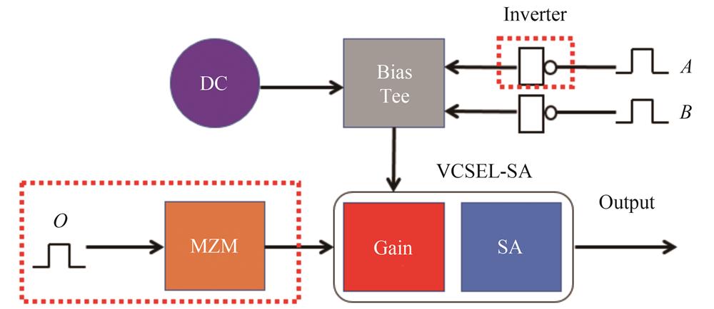
    Fig. 1. Schematic diagram of photoelectric logic gate(NOT,NAND,NOR,XOR)based on VCSEL-SA
    The output of the VCSEL-SA for different modulation signal amplitude
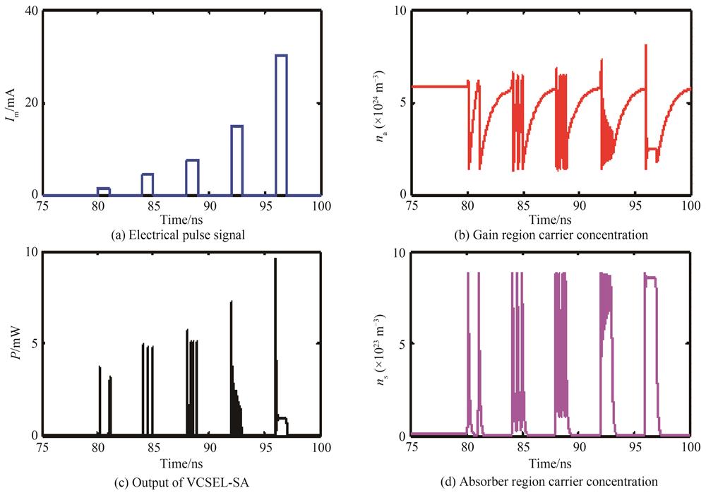
    Fig. 2. The output of the VCSEL-SA for different modulation signal amplitude
    The output of the VCSEL-SA for modulation signals with different perturbation durations
    Fig. 3. The output of the VCSEL-SA for modulation signals with different perturbation durations
    Output of VCSEL-SA under external disturbance
    Fig. 4. Output of VCSEL-SA under external disturbance
    Implementation of NOT logic operation
    Fig. 5. Implementation of NOT logic operation
    Logic operation implementation of NAND gate and NOR gate
    Fig. 6. Logic operation implementation of NAND gate and NOR gate
    Implementation of XOR logic operation
    Fig. 7. Implementation of XOR logic operation
    Evolution of the VCSEL-SA's output with Im
    Fig. 8. Evolution of the VCSEL-SA's output with Im
    Influence of the input delay between two current modulation signals on the optoelectronic logic gate(NAND,NOR)
    Fig. 9. Influence of the input delay between two current modulation signals on the optoelectronic logic gate(NAND,NOR)
    The effect of noise on the implementation of optoelectronic logic gates(NAND,NOR,XOR)
    Fig. 10. The effect of noise on the implementation of optoelectronic logic gates(NAND,NOR,XOR)
    ParameterDescriptionValue
    ΓaConfinement factor in active region0.06
    ΓsConfinement factor in absorber region0.05
    τaCarrier lifetime in gain region/ns1
    τsCarrier lifetime in absorber region/ps100
    τphPhoton lifetime/ps4.8
    hPlanck constant/(J·s)6.634×10-34
    VaGain region volume/m32.4×10-18
    VsAbsorber region volume/m32.4×10-18
    cSpeed of light/(m·s-13×108
    gaDifferential gain/loss in gain region/(m3·s-12.9×10-12
    gsDifferential gain/loss in absorber region/(m3·s-114.5×10-12
    n0aTransparency carrier density in gain region/m-31.1×1024
    n0sTransparency carrier density in absorber region/m-30.89×1024
    BrBimolecular recombination factor/(m3·s-11×10-15
    βSpontaneous emission coupling factor1×10-4
    ηcOutput power coupling coefficient0.4
    IsBias current in absorber region/mA0
    λLaser wavelength/nm850
    Table 1. Typical VCSEL-SA parameters
    Luyao XIAO, Xi TANG, Xiaodong LIN, Ziye GAO, Zhifei DUAN, Xiaorui DU, Guangqiong XIA, Zhengmao WU, Tao DENG. Reconfigurable Logic Operation Based on Optically Injected VCSEL-SA Subject to Current Modulation[J]. Acta Photonica Sinica, 2022, 51(11): 1114005
    Download Citation