We present compact silicon-arrayed waveguide grating routers (AWGRs) with three different channel spacings of 20, 6.4, and 3.2 nm for optical interconnect systems. The AWGR with the 20 nm channel spacing shows a low loss of 2.5 dB and a low crosstalk of and has a footprint of only . The AWGR with the channel spacing of 6.4 nm has loss ranging from 3 to 8 dB, and the crosstalk is . As for the 3.2 nm channel spacing, the loss is about 4 dB, and the crosstalk is .
With the rapid increase of bandwidth requirements, traditional electrical interconnects are facing an inevitable bottleneck in data center traffic. In the meantime, optical interconnect systems based on wavelength division multiplexing (WDM) provide many advantages, such as a large bandwidth and low power consumption[1]. Wavelength routers are key components in WDM optical interconnect systems. For example, arrayed waveguide gratings (AWGs) can route 16 channels with 4 different wavelengths at the same time, which means the bandwidth and data throughput would be improved significantly compared with electro-optical switches[2]. AWG routers (AWGRs) have been demonstrated in many material systems, such as silica, polymer, and InP[3–5], and show good performance. The development of silicon-on-insulator (SOI) technology has enabled ultra-compact silicon photonic integrated circuits because of the large refractive index contrast between silicon and silica[6]. Therefore, SOI-based AWGRs have drawn more and more attention recently. In 2014, Wang et al. demonstrated an AWGR that showed a crosstalk of and insertion loss of [7]. A 25 GHz AWGR with a crosstalk of was experimentally demonstrated[8]. In addition, an AWGR with a channel spacing of 400 GHz based on parabolic tapers was reported in 2014 and showed a low crosstalk of about [9]. In 2015, Li et al. demonstrated and AWGs with crosstalk of and 21.4 dB. The devices size were μμ and μμ, respectively[10]. In this Letter, we design and fabricate ultra-compact AWGRs with several different channel spacings for coarse WDM (CWDM) or dense WDM (DWDM) systems. The devices are characterized and show good performances, with low insertion loss and crosstalk.
The basic diffraction equation for AWGs based on the Rowland circle construction can be expressed as with and effective as the refractive indices of the free propagation region (FPR) and arrayed waveguides, respectively, as the distance between adjacent arrayed waveguides at the FPR interface, as the incident angle from one of the four input waveguides, and as the output angles at a certain demultiplexing wavelength. is the length difference between adjacent arrayed waveguides, is the diffraction order, and is the wavelength in a vacuum. To realize optical routing, two adjacent diffraction orders should be connected without a gap. As a result, the free spectral range (FSR) is times the channel spacing , where is the group index of the arrayed waveguide, and is the central wavelength.
In this Letter, we used an SOI wafer with a 220 nm silicon core layer and a 2 μm under cladding layer. For single-mode operation, the width of the arrayed waveguides is chosen to be 500 nm. First, we take a AWGR with a channel spacing of 20 nm for TM operation as an example. Table 1 shows the main parameters of the AWGR, and the footprint of the device is only .
Sign up for Chinese Optics Letters TOC. Get the latest issue of Chinese Optics Letters delivered right to you!Sign up now
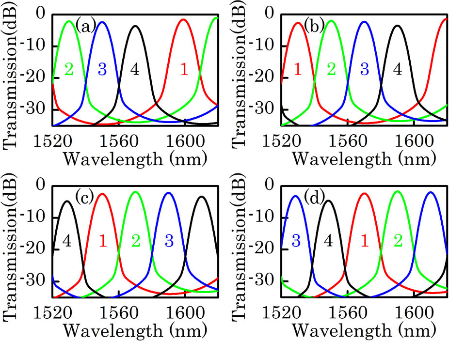
Figure 1 shows the simulation results of the AWGR based on the Kirchhoff−Huygens diffraction law. The simulated spectra show insertion loss non-uniformity due to the power conservation[11]. To reduce the non-uniformity of the insertion loss, extra input and output waveguides are required, and the waveguides on the output side are combined through waveguide intersections and multimode interference couplers to make output ports[12]. But there is still a 3 dB loss budget in the optical combiner, and the footprint of the device is quite large. What is more, the simulated wavelengths of several output channels are slightly different from the intended values because edge output channels belong to adjacent diffraction orders whose FSRs and channel spacings are slightly different.
Figure 1.Simulated spectral responses of (a) first input channel, (b) second input channel, (c) third input channel, and (d) fourth input channel.
As for fabrication, a standard SOI wafer with a 220 nm silicon core layer and a 2 μm buried oxide layer from SOITEC was used to fabricate the AWGR. In the first step, a thin hard mask was deposited on the wafer by plasma-enhanced chemical vapor deposition (PECVD). Then, we spin-coated the negative photoresist (maN-2403) onto the film. The pattern of the AWGR was written by electron-beam lithography. After development, the mask was etched by inductive coupled plasma reactive ion etching (ICP-RIE) to transfer the pattern from the photoresist. Another process of ICP-RIE was carried out to etch through the silicon core layer. Subsequently, the remaining photoresist was removed with a mixed solution consisting of and . Last, a 1.5 μm thick film was deposited by PECVD on the wafer as the upper cladding layer. The wafer was cleaved into small chips for the test. Figure 2(a) is the scanning electron microscope image of the fabricated AWGR. As shown in Fig. 2(b), linear tapers were used to reduce the mode transition mismatch between the FPR and arrayed waveguides.
Figure 2.(a) Scanning electron microscope images of the fabricated AWGR and (b) tapers between the FPR and arrayed waveguides.
To characterize the AWGR, a polarization-maintaining lensed fiber is used to couple the quasi-TM light from a tunable laser (Agilent 81600B) to input the waveguides of the AWGR through one facet of the chip. A polarization controller is used to control the polarization of the input light. Light from the output waveguides of the AWGR is coupled to another lensed fiber and received by a power sensor (Agilent 81635A).
The measured transmission spectra are presented in Fig. 3. Due to the width deviation and phase error of the fabricated arrayed waveguides, the central wavelength and FSR show slight differences from the design values of 1550 and 80 nm, respectively. After being normalized to a reference straight waveguide, the insertion loss varies from 2.5 to 5 dB, which agrees well with the simulation results. The measured crosstalk is better than . As can be seen in Fig. 3, the AWGR shows a good cyclic rotation function and can be applied in CWDM interconnection systems.
Figure 3.Measured spectral responses of (a) first input channel, (b) second input channel, (c) third input channel, and (d) fourth input channel.
In addition, silicon nanowire AWGRs with channel spacings of 6.4 and 3.2 nm for DWDM applications are also demonstrated. Table 1 shows the main parameters.
To couple light to on-chip devices more efficiently, we apply grating couplers for TM polarization. The pitch of the grating couplers is 990 nm, the duty cycle is 0.7, and the etch depth is 220 nm, which requires only a single etching step[13]. The lowest coupling loss between the grating coupler and fiber is 5 dB at 1550 nm. As for fabrication, the same process as mentioned was carried out, except for the cleaving step.
After normalized to a reference straight waveguide, the measured transmission spectra of the AWGR with a 6.4 nm channel spacing for the center and edge channel inputs are shown in Figs. 4 and 5, respectively. As can be seen, a low insertion loss of 3 dB and a low crosstalk of are obtained. The channel spacing and FSR are in good agreement with designed values. After measuring the spectra of all 8×8 channels, the insertion losses of all channels are shown in Fig. 6 and range from 3.15 to 8.17 dB.
Figure 4.Measured transmission spectrum of the center input channel of the AWGR with the 6.4 nm channel spacing.
The measured transmission spectrum of the center input channel of the AWGR with a 3.2 nm channel spacing is shown in Fig. 7. The crosstalk of the 3.2 nm AWGR is relatively higher than that of the 6.4 nm AWGR because of larger phase error resulting from the larger chip size. The effect of the non-uniform silicon core layer is more severe when the channel spacing becomes smaller and the FPR becomes larger.
Figure 7.Measured transmission spectrum of the center input channel of the AWGR with the 3.2 channel spacing.
For comparison, Table 2 shows the number of channels, channel spacings, insertion losses, and crosstalk performance of the reported AWGRs on the SOI platform. As can be seen, our devices show good performances considering both the number of channels and channel spacings.
In conclusion, we design and fabricate ultra-compact AWGRs with three different channel spacings from 20 to 3.2 nm based on silicon nanowires. The devices have a small footprint and achieve a high performance, with low insertion losses (2.5–5 dB) and low crosstalk (). The Si nanowire AWGRs also show a good cyclic rotation function and can be applied in CWDM or DWDM optical interconnect systems. With such a small footprint, the AWGRs can be integrated with other optical devices and packaged for module applications.
Reference
Number of channel
Channel spacing (nm)
Loss (dB)
Crosstalk (dB)
[5]
8
0.8
2.92
−16.9–17.8
[6]
512
0.2
11.3
−4
[7]
8
3.2
2.4
−17.6–25.1
This work
4
20
2.5
−20
This work
8
6.4
3
−18
This work
16
3.2
4.9
−12
Table 2. Comparison of Reported AWGRs on SOI Platform with Devices in this Work