• Acta Physica Sinica
  • Vol. 68, Issue 22, 227102-1 (2019)
Tao Deng1、2、3, Hai-Feng Yang3, Jing Zhang3, Yi-Wei Li4, Le-Xian Yang5, Zhong-Kai Liu3、*, and Yu-Lin Chen3、4、5、*
Author Affiliations
  • 1CAS Center for Excellence in Superconducting Electronics (CENSE), State Key Laboratory of Functional Materials for Informatics, Shanghai Institute of Microsystem and Information Technology (SIMIT), Chinese Academy of Sciences, Shanghai 200050, China
  • 2University of Chinese Academy of Sciences, Beijing 100049, China
  • 3School of Physical Science and Technology, ShanghaiTech University, ShanghaiTech Laboratory for Topological Physics, Shanghai 201210, China
  • 4Department of Physics, University of Oxford, Oxford OX1 3PU, United Kingdom
  • 5Department of Physics, Tsinghua University, Beijing 100084, China
  • show less
    DOI: 10.7498/aps.68.20191544 Cite this Article
    Tao Deng, Hai-Feng Yang, Jing Zhang, Yi-Wei Li, Le-Xian Yang, Zhong-Kai Liu, Yu-Lin Chen. Progress of ARPES study on topological semimetals[J]. Acta Physica Sinica, 2019, 68(22): 227102-1 Copy Citation Text show less
    (a) Illustration of a photoemission experiment; (b) curve of electric IMFP vs energy; (c) energetics of the photoemission process; (d) illustration different FSs measured by ARPES under different photon energies due to the kz dispersion in k-space of a 3D Fermi Surface.(a)光电子能谱实验原理示意图; (b)光电子非弹性平均自由程与能量关系图; (c)光电效应过程的能量关系图示; (d) ARPES测量不同kz等能面示意图
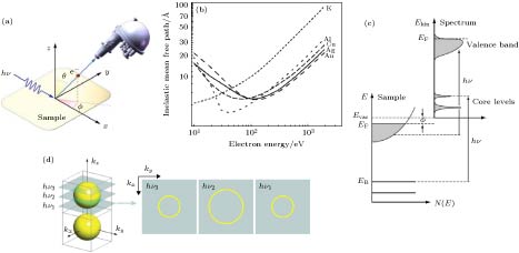
    Fig. 1. (a) Illustration of a photoemission experiment; (b) curve of electric IMFP vs energy; (c) energetics of the photoemission process; (d) illustration different FSs measured by ARPES under different photon energies due to the kz dispersion in k-space of a 3D Fermi Surface. (a)光电子能谱实验原理示意图; (b)光电子非弹性平均自由程与能量关系图; (c)光电效应过程的能量关系图示; (d) ARPES测量不同kz等能面示意图
    A picture of the synchrotron-based nano-ARPES workstation in SSRF BL03U.上海光源中同步辐射束线BL03U搭载的空间分辨角分辨光电子能谱实验工作站图
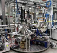
    Fig. 2. A picture of the synchrotron-based nano-ARPES workstation in SSRF BL03U.上海光源中同步辐射束线BL03U搭载的空间分辨角分辨光电子能谱实验工作站图
    (a) Illustration of a 3D Dirac Fermion in 4D energy-momentum space and its projection onto different 3D subspace; (b) the crystal structure of Na3Bi; (c) 1st Brillouin zone of Na3Bi; (d) measured Fermi surface map across the whole 3D BZ (top panel) and its projection on the surface BZ (bottom panel) on pristine surfaces. 3D intensity plot of the photoemission spectra (e) along the kDy–kDx direction and (f) along the kDy–kDz direction at the Dirac point.(a)三维狄拉克费米子在能-动量四维空间示意图及其在不同三维能-动量子空间的投影; (b) Na3Bi的晶体结构示意图; (c) Na3Bi的第一布里渊区示意图; (d)在三维动量空间中的实验测量费米面(上半图)及其在表面布里渊区的投影(下半图) (e) (f)狄拉克点处沿kDy–kDx和kDy–kDz方向的三维光电子谱图
    Fig. 3. (a) Illustration of a 3D Dirac Fermion in 4D energy-momentum space and its projection onto different 3D subspace; (b) the crystal structure of Na3Bi; (c) 1st Brillouin zone of Na3Bi; (d) measured Fermi surface map across the whole 3D BZ (top panel) and its projection on the surface BZ (bottom panel) on pristine surfaces. 3D intensity plot of the photoemission spectra (e) along the kDy–kDx direction and (f) along the kDykDz direction at the Dirac point. (a)三维狄拉克费米子在能-动量四维空间示意图及其在不同三维能-动量子空间的投影; (b) Na3Bi的晶体结构示意图; (c) Na3Bi的第一布里渊区示意图; (d)在三维动量空间中的实验测量费米面(上半图)及其在表面布里渊区的投影(下半图) (e) (f)狄拉克点处沿kDykDxkDykDz方向的三维光电子谱图
    (a) Schematic of Fermi surface in Na3Bi cleaved along (100) direction; (b) Fermi surface measured by ARPES experiment; (c) spectrum cut along α from (b); (d) theoretical calculated spin texture of Fermi arcs; (e) band structure along ; (f) calculated projected bands corresponding to (c) when ky = 0.(a)沿(100)解理的Na3Bi费米面示意图; (b) ARPES实验测得的费米面图像; (c)图(b)中沿α方向切出的能谱; (d)费米弧的理论自旋织构图; (e)沿方向的能带结构图; (f) ky = 0时图(c)对应的方向理论计算投影能谱
    Fig. 4. (a) Schematic of Fermi surface in Na3Bi cleaved along (100) direction; (b) Fermi surface measured by ARPES experiment; (c) spectrum cut along α from (b); (d) theoretical calculated spin texture of Fermi arcs; (e) band structure along ; (f) calculated projected bands corresponding to (c) when ky = 0. (a)沿(100)解理的Na3Bi费米面示意图; (b) ARPES实验测得的费米面图像; (c)图(b)中沿α方向切出的能谱; (d)费米弧的理论自旋织构图; (e)沿 方向的能带结构图; (f) ky = 0时图(c)对应的 方向理论计算投影能谱
    3D visualization of type-II Dirac cone: (a) Schematic of type-II Dirac cone projected on kx-ky-E space; (b) 3D ARPES map (hν = 24 eV) which slices through the type-II BDP (pointed out by magenta arrow); (c) zoomed-in ARPES constant energy contours (CECs) of Fig.(b); (d) schematic of type-II Dirac cone projected on kx–kz–E space; (e) 3D kz-dependent map (hν = 18–33 eV); (f) zoomed-in ARPES CECs of Fig. (e).第二类狄拉克锥的三维示意图 (a)投影在kx–ky–E空间上的第二类狄拉克锥简图; (b) PtSe2中kx–ky面内切过第二类体狄拉克点的三维色散能谱图(光能24 eV), 狄拉克点由紫色箭头指出; (c)放大的图(b)中ARPES等能面堆叠图; (d)投影在ky–kz–E空间上的第二类狄拉克锥简图; (e)三维kz依赖的色散能谱图(光能18—33 eV); (f)放大的图(e)中ARPES等能面堆叠图
    Fig. 5. 3D visualization of type-II Dirac cone: (a) Schematic of type-II Dirac cone projected on kx-ky-E space; (b) 3D ARPES map (hν = 24 eV) which slices through the type-II BDP (pointed out by magenta arrow); (c) zoomed-in ARPES constant energy contours (CECs) of Fig.(b); (d) schematic of type-II Dirac cone projected on kxkzE space; (e) 3D kz-dependent map ( = 18–33 eV); (f) zoomed-in ARPES CECs of Fig. (e). 第二类狄拉克锥的三维示意图 (a)投影在kxkyE空间上的第二类狄拉克锥简图; (b) PtSe2kxky面内切过第二类体狄拉克点的三维色散能谱图(光能24 eV), 狄拉克点由紫色箭头指出; (c)放大的图(b)中ARPES等能面堆叠图; (d)投影在kykzE空间上的第二类狄拉克锥简图; (e)三维kz依赖的色散能谱图(光能18—33 eV); (f)放大的图(e)中ARPES等能面堆叠图
    (a) Crystal structure (with its top view) and (b) 1st Brillouin zone (with surface BZ marked in blue) of PtTe2; (c) (d) evolution of crystal-field-derived levels with the out-of-plane kz momentum when hybridization is (c)neglected or (d)included, showing a protected crossing of the A1 and E-derived levels; (e) ARPES spectrum along Γ-A-Γ direction (kz corresponding to hv = 80−132 eV) with calculated bands (yellow lines) attached; (f) ARPES spectrum alongdirection (hv = 27 eV); (g) calculated energy bands projected on surface Brillouin zone.(a) PdTe2型材料的晶体结构(及其俯视图)和(b)第一布里渊区(蓝色所示为(001)表面布里渊区); (c)忽略杂化和(d)考虑杂化时晶体场产生的能级随kz动量变化的演化, A1与E产生的能级在绿点处出现受保护的交界点; (e)沿Γ-A-Γ方向的ARPES能谱(横轴为光能80−132 eV对应的kz区间), 黄线为理论计算的能带; (f)沿表面布里渊区方向的ARPES能谱(光能27 eV), 小图为24 eV时的局部放大图; (g)理论计算的表面布里渊区能带投影图
    Fig. 6. (a) Crystal structure (with its top view) and (b) 1st Brillouin zone (with surface BZ marked in blue) of PtTe2; (c) (d) evolution of crystal-field-derived levels with the out-of-plane kz momentum when hybridization is (c)neglected or (d)included, showing a protected crossing of the A1 and E-derived levels; (e) ARPES spectrum along Γ-A-Γ direction (kz corresponding to hv = 80−132 eV) with calculated bands (yellow lines) attached; (f) ARPES spectrum along direction (hv = 27 eV); (g) calculated energy bands projected on surface Brillouin zone. (a) PdTe2型材料的晶体结构(及其俯视图)和(b)第一布里渊区(蓝色所示为(001)表面布里渊区); (c)忽略杂化和(d)考虑杂化时晶体场产生的能级随kz动量变化的演化, A1E产生的能级在绿点处出现受保护的交界点; (e)沿Γ-A-Γ方向的ARPES能谱(横轴为光能80−132 eV对应的kz区间), 黄线为理论计算的能带; (f)沿表面布里渊区 方向的ARPES能谱(光能27 eV), 小图为24 eV时的局部放大图; (g)理论计算的表面布里渊区能带投影图
    (a) Crystal structure of TaAs; (b) schematic of a WSM electronic structure with spin-polarized Fermi arcs connecting projections of two bulk Weyl nodes (The red and blue colors represent opposite chirality. For clarity, only surface states on the top and bottom surfaces are indicated); (c) (i) calculated position of Weyl Fermions and Fermi arcs in 1st BZ with its (ii) top view; (iii) shows the photoemission intensity plot at EF in the ky–kz plane at kx = 0 (The green lines represent the BZ structure in the ky–kz plane.); (d) Fermi surface measured by ARPES experiment (hv = 36 eV); (e) illustration of band numbers crossing an arbitrary k loop. Blue and magenta circles indicate the locations where the bands cross the enclosed k loop and at EF, respectively. (f) zoomed-in experimental and theoretical Fermi surface near W1 Weyl point (spin polarizations of Fermi arc marked by red arrows); (g) theoretical spin texture of surface states on Fermi surface (spin polarization indicated by white arrows); (h) angle-resolved spin polarizations along C1, C2 (marked in Fig. (g) with white lines) in the z direction.(a) TaAs的晶体结构; (b)有自旋极化费米弧的外尔半金属电子结构图示(红色和蓝色分别代表不同的手性. 为清晰起见, 图中只画出了顶面和底面的表面态); (c)理论计算的第一布里渊区中外尔费米子及费米弧位置及其(ii)俯视图, (iii)为费米能级处ky–kz面上(kx = 0)光电子强度谱的等能面能谱, 绿线为ky–kz面上的布里渊区边线; (d)ARPES实验(光能36 eV)所得的kx–ky费米面; (e)选取闭合路径计算能带穿越费米面数目的示意图, 紫色及蓝色圆点代表能带穿越和闭合回路的位置; (f)费米面上W1外尔点附近理论计算的局部放大图; (g)理论计算的费米面上表面态自旋织构(白色箭头为面内自旋极化方向); (h)沿图(g)中C1, C2在Pz方向的角分辨自旋极化情况
    Fig. 7. (a) Crystal structure of TaAs; (b) schematic of a WSM electronic structure with spin-polarized Fermi arcs connecting projections of two bulk Weyl nodes (The red and blue colors represent opposite chirality. For clarity, only surface states on the top and bottom surfaces are indicated); (c) (i) calculated position of Weyl Fermions and Fermi arcs in 1st BZ with its (ii) top view; (iii) shows the photoemission intensity plot at EF in the kykz plane at kx = 0 (The green lines represent the BZ structure in the kykz plane.); (d) Fermi surface measured by ARPES experiment (hv = 36 eV); (e) illustration of band numbers crossing an arbitrary k loop. Blue and magenta circles indicate the locations where the bands cross the enclosed k loop and at EF, respectively. (f) zoomed-in experimental and theoretical Fermi surface near W1 Weyl point (spin polarizations of Fermi arc marked by red arrows); (g) theoretical spin texture of surface states on Fermi surface (spin polarization indicated by white arrows); (h) angle-resolved spin polarizations along C1, C2 (marked in Fig. (g) with white lines) in the z direction. (a) TaAs的晶体结构; (b)有自旋极化费米弧的外尔半金属电子结构图示(红色和蓝色分别代表不同的手性. 为清晰起见, 图中只画出了顶面和底面的表面态); (c)理论计算的第一布里渊区中外尔费米子及费米弧位置及其(ii)俯视图, (iii)为费米能级处kykz面上(kx = 0)光电子强度谱的等能面能谱, 绿线为kykz面上的布里渊区边线; (d)ARPES实验(光能36 eV)所得的kxky费米面; (e)选取闭合路径计算能带穿越费米面数目的示意图, 紫色及蓝色圆点代表能带穿越 和 闭合回路的位置; (f)费米面上W1外尔点附近理论计算的局部放大图; (g)理论计算的费米面上表面态自旋织构(白色箭头为面内自旋极化方向); (h)沿图(g)中C1, C2在Pz方向的角分辨自旋极化情况
    Observation of bulk Weyl cones and Weyl nodes in TaAs using SX-ARPES: (a) Measured and first principles calculated kx-ky Fermi surface maps at the kz value that corresponds to the W1 Weyl nodes; (b) ARPES spectra cut along (i)cut1 and (ii)cut2 from Fig. (a); (c) measured kx-ky Fermi surface maps at the kz value that corresponds to the W2 Weyl nodes as well as the spectrum cut along cut3. Linearly dispersive Weyl cones of both W1 and W2 can be observed.软X射线ARPES下TaAs中体外尔锥和外尔点观测图 (a) kz穿过外尔点W1时候采得的费米面及其理论简图; (b) (i)沿图(a)中cut1, cut2方向切出的角分辨光电子能谱图; (c) kz穿过外尔点W2时候采得的费米面及沿cut3方向切出的能谱; 过外尔点W1, W2均可看到线性色散外尔锥
    Fig. 8. Observation of bulk Weyl cones and Weyl nodes in TaAs using SX-ARPES: (a) Measured and first principles calculated kx-ky Fermi surface maps at the kz value that corresponds to the W1 Weyl nodes; (b) ARPES spectra cut along (i)cut1 and (ii)cut2 from Fig. (a); (c) measured kx-ky Fermi surface maps at the kz value that corresponds to the W2 Weyl nodes as well as the spectrum cut along cut3. Linearly dispersive Weyl cones of both W1 and W2 can be observed. 软X射线ARPES下TaAs中体外尔锥和外尔点观测图 (a) kz穿过外尔点W1时候采得的费米面及其理论简图; (b) (i)沿图(a)中cut1, cut2方向切出的角分辨光电子能谱图; (c) kz穿过外尔点W2时候采得的费米面及沿cut3方向切出的能谱; 过外尔点W1, W2均可看到线性色散外尔锥
    (a) Illustration of the separation of Weyl points (with opposite chirality, marked as WP+ and WP–) in different materials of TaAs family with increasing spin-orbital coupling effect; (b)–(d) high-resolution ARPES measurements on the (i) spoon-like FS and (ii, iii) associated band dispersions indicated by the red dotted lines for NbP, TaP and TaAs, respectively (ΔK1 and ΔK2 represent the separation between the Weyl points and Fermi arcs, respectively.); (e) summary of the extracted ΔK1 and ΔK2 from the three compounds, plotted against the SOC strength(a) TaAs家族中不同自旋轨道耦合强度材料中手性相反外尔点的位置演化图; (b)—(d)高分辨ARPES测量的NbP, TaP和TaAs的(i)勺状费米面以及(ii) (iii)沿C1, C2红虚线方向的能谱; (ΔK1和ΔK2分布代表外尔点、费米弧的分离程度); (e)统计得到的ΔK1和ΔK2随三种不同材料自旋轨道耦合强度变化图像
    Fig. 9. (a) Illustration of the separation of Weyl points (with opposite chirality, marked as WP+ and WP–) in different materials of TaAs family with increasing spin-orbital coupling effect; (b)–(d) high-resolution ARPES measurements on the (i) spoon-like FS and (ii, iii) associated band dispersions indicated by the red dotted lines for NbP, TaP and TaAs, respectively (ΔK1 and ΔK2 represent the separation between the Weyl points and Fermi arcs, respectively.); (e) summary of the extracted ΔK1 and ΔK2 from the three compounds, plotted against the SOC strength (a) TaAs家族中不同自旋轨道耦合强度材料中手性相反外尔点的位置演化图; (b)—(d)高分辨ARPES测量的NbP, TaP和TaAs的(i)勺状费米面以及(ii) (iii)沿C1, C2红虚线方向的能谱; (ΔK1和ΔK2分布代表外尔点、费米弧的分离程度); (e)统计得到的ΔK1和ΔK2随三种不同材料自旋轨道耦合强度变化图像
    Magnetic Weyl semimetal Co3Sn2S2: (a) Exotic neighboring states of the magnetic WSM can be achieved by tuning parameters such as magnetism, thickness, and electron correlation; (b) illustration of DP splitting (into one pair or two Weyl points) caused by time reversal symmetry broken in simplest magnetic WSMs. Magenta and green color of the Weyl points represent positive (+) and negative (–) chirality, respectively; the arrows illustrate the Berry curvature. k: momentum; s: spin; WP: Weyl point; IS: inversion symmetry; (c) crystal structure of Co3Sn2S2 and (d) schematic of the bulk and surface Brillouin zones along the (001) surface of Co3Sn2S2, with the Weyl points marked and connected by SFAs (yellow line segments); (e) comparison of the calculated (i) FS, (iii) band dispersion from both bulk and surface states and the corresponding experimental data of (ii) FS, (iv) band dispersion at 124 eV; (f) (i) 3D ARPES spectra intensity plot measured with Weyl points emerge (marked by green arrows). (ii) The band measured at 10 K, cutting from (i) with grey surface, shows a linear dispersion across the Weyl point, agreeing well with the calculations (red curves overlaid).磁性Weyl半金属Co3Sn2S2 (a)磁性Weyl半金属及其丰富的近邻量子态; (b)时间反演破缺使狄拉克费米子(DP)劈裂产生一对手性相反的外尔费米子(WP)示意图; (c) Co3Sn2S2晶体结构及(d)动量空间中(001)面外尔点和费米弧表面态分布示意图; (e)费米弧表面态所形成费米面的理论计算(i)和实验结果(ii)比较以及费米弧表面态能带色散的理论计算(iii)和实验结果(iv)比较; (f)费米面上的Weyl点(i)及其能带(ii)的三维演示; (ii)中过Weyl点的线性色散为(i)中灰色平面位置所切取, 红色的叠加曲线是理论计算结果
    Fig. 10. Magnetic Weyl semimetal Co3Sn2S2: (a) Exotic neighboring states of the magnetic WSM can be achieved by tuning parameters such as magnetism, thickness, and electron correlation; (b) illustration of DP splitting (into one pair or two Weyl points) caused by time reversal symmetry broken in simplest magnetic WSMs. Magenta and green color of the Weyl points represent positive (+) and negative (–) chirality, respectively; the arrows illustrate the Berry curvature. k: momentum; s: spin; WP: Weyl point; IS: inversion symmetry; (c) crystal structure of Co3Sn2S2 and (d) schematic of the bulk and surface Brillouin zones along the (001) surface of Co3Sn2S2, with the Weyl points marked and connected by SFAs (yellow line segments); (e) comparison of the calculated (i) FS, (iii) band dispersion from both bulk and surface states and the corresponding experimental data of (ii) FS, (iv) band dispersion at 124 eV; (f) (i) 3D ARPES spectra intensity plot measured with Weyl points emerge (marked by green arrows). (ii) The band measured at 10 K, cutting from (i) with grey surface, shows a linear dispersion across the Weyl point, agreeing well with the calculations (red curves overlaid). 磁性Weyl半金属Co3Sn2S2  (a)磁性Weyl半金属及其丰富的近邻量子态; (b)时间反演破缺使狄拉克费米子(DP)劈裂产生一对手性相反的外尔费米子(WP)示意图; (c) Co3Sn2S2晶体结构及(d)动量空间中(001)面外尔点和费米弧表面态分布示意图; (e)费米弧表面态所形成费米面的理论计算(i)和实验结果(ii)比较以及费米弧表面态能带色散的理论计算(iii)和实验结果(iv)比较; (f)费米面上的Weyl点(i)及其能带(ii)的三维演示; (ii)中过Weyl点的线性色散为(i)中灰色平面位置所切取, 红色的叠加曲线是理论计算结果
    (a) Schematic illustration of type-II Weyl Fermions in the momentum space; (b) crystal structure and (c) 1st Brillouin zone of Td-MoTe2; (d) calculated W1 and W2 Weyl Fermions and Fermi arcs on CECs; (e) (i) photon-energy dependent ARPES data (T = 30 K) plot along at EF as well as Fermi surface in the kx–ky plane, together with (iii) spin polarization measured at ky ≈ 0.05 Å–1 with photon-energy variation for Px, Py and Pz, respectively. EPs, HPs are short for electron pockets and hole pockets, small Fermi arcs are pointed out by α, β, γ, δ dashed lines; (f) measured and calculated Fermi surface around W1 and W2 in kx–ky plane; (g) pump-probe ARPES sprectrum cut through WP as well as the corresponding band structure calculation.(a)第二类外尔费米子在动量空间中示意图; (b) Td-MoTe2的晶体结构及其(c)第一布里渊区示意图; (d)理论计算的W1和W2外尔费米子及费米弧在等能面上的位置; (e) (i)温度30 K下沿方向的光能依赖ARPES谱以及(ii)kx-ky面上的EF处等能面谱图, (iii)在ky ≈ 0.05 Å–1处沿Px, Py和Pz方向的光能依赖自旋极化情况(表示电子口袋和空穴口袋的EPs和HPs以及费米弧等由α, β, γ, δ等虚线指出); (f)kx–ky面内W1和W2外尔点附近的实验费米面图像及理论计算能带投影图; (g)利用泵浦-探测技术测得的过外尔点ARPES谱图及其对应的理论计算结果
    Fig. 11. (a) Schematic illustration of type-II Weyl Fermions in the momentum space; (b) crystal structure and (c) 1st Brillouin zone of Td-MoTe2; (d) calculated W1 and W2 Weyl Fermions and Fermi arcs on CECs; (e) (i) photon-energy dependent ARPES data (T = 30 K) plot along at EF as well as Fermi surface in the kxky plane, together with (iii) spin polarization measured at ky ≈ 0.05 Å–1 with photon-energy variation for Px, Py and Pz, respectively. EPs, HPs are short for electron pockets and hole pockets, small Fermi arcs are pointed out by α, β, γ, δ dashed lines; (f) measured and calculated Fermi surface around W1 and W2 in kxky plane; (g) pump-probe ARPES sprectrum cut through WP as well as the corresponding band structure calculation. (a)第二类外尔费米子在动量空间中示意图; (b) Td-MoTe2的晶体结构及其(c)第一布里渊区示意图; (d)理论计算的W1和W2外尔费米子及费米弧在等能面上的位置; (e) (i)温度30 K下沿 方向的光能依赖ARPES谱以及(ii)kx-ky面上的EF处等能面谱图, (iii)在ky ≈ 0.05 Å–1处沿Px, PyPz方向的光能依赖自旋极化情况(表示电子口袋和空穴口袋的EPs和HPs以及费米弧等由α, β, γ, δ等虚线指出); (f)kxky面内W1和W2外尔点附近的实验费米面图像及理论计算能带投影图; (g)利用泵浦-探测技术测得的过外尔点ARPES谱图及其对应的理论计算结果
    Crystal structure and band structure of MoP along the Γ–A line in the momentum space: (a) Three-dimensional crystal structure of MoP and (b) the top view of the lattice showing the C3Z rotation symmetry with respect to molybdenum (brown spheres) or phosphorous (green spheres) and the My mirror plane (horizontal red line); (c) bulk Brillouin zone and the projected (001) surface Brillouin zone; (d) (e) calculated band structures along Γ–A (d) without and (e) with SOC. The black spots at the crossing points indicate the triply degenerate points. The curves with mixed colors represent doubly degenerate bands, curves with pure color represent non-degenerate bands.MoP的晶体结构及动量空间Γ—A方向能带结构图示 (a) MoP的三维晶体结构及(b) Mz方向(黄色面)俯视图; (c)体布里渊区和投影的(001)表面布里渊区; (d)不考虑及(e)考虑自旋轨道耦合时沿Γ—A方向的理论能带结构. 交叉点处的黑点表示三重简并点. 颜色混合标注的曲线表示双重简并能带, 纯色曲线表示非简并带
    Fig. 12. Crystal structure and band structure of MoP along the ΓA line in the momentum space: (a) Three-dimensional crystal structure of MoP and (b) the top view of the lattice showing the C3Z rotation symmetry with respect to molybdenum (brown spheres) or phosphorous (green spheres) and the My mirror plane (horizontal red line); (c) bulk Brillouin zone and the projected (001) surface Brillouin zone; (d) (e) calculated band structures along ΓA (d) without and (e) with SOC. The black spots at the crossing points indicate the triply degenerate points. The curves with mixed colors represent doubly degenerate bands, curves with pure color represent non-degenerate bands. MoP的晶体结构及动量空间ΓA方向能带结构图示 (a) MoP的三维晶体结构及(b) Mz方向(黄色面)俯视图; (c)体布里渊区和投影的(001)表面布里渊区; (d)不考虑及(e)考虑自旋轨道耦合时沿ΓA方向的理论能带结构. 交叉点处的黑点表示三重简并点. 颜色混合标注的曲线表示双重简并能带, 纯色曲线表示非简并带
    Electronic structure near TP1. (a)-(c) (i) ARPES, (ii) curvature intensity plots and (iii)calculated band structure along (a) C1, (b) C2 and (c) C3; (C1, C2, C3 are blue and green lines indicated in (d)) (e) 3D plot of the band dispersions along C1 near TP1. Spectrum along C1 is recorded on the (100) cleavage surface; those along C2 and C3 are obtained on the (001) cleavage surface.拓扑简并点TP1附近的电子结构 (a)—(c)沿C1, C2, C3方向((i)—(iii))的ARPES及其能带曲率谱图与理论计算能带色散; (d) C1, C2, C3方向在体布里渊区中的位置示意图; (e)沿C1演化的TP1点附近能带分布三维色散图. C1能谱由(100)解理面采得而C2, C3由(001)解理面采得
    Fig. 13. Electronic structure near TP1. (a)-(c) (i) ARPES, (ii) curvature intensity plots and (iii)calculated band structure along (a) C1, (b) C2 and (c) C3; (C1, C2, C3 are blue and green lines indicated in (d)) (e) 3D plot of the band dispersions along C1 near TP1. Spectrum along C1 is recorded on the (100) cleavage surface; those along C2 and C3 are obtained on the (001) cleavage surface.拓扑简并点TP1附近的电子结构  (a)—(c)沿C1, C2, C3方向((i)—(iii))的ARPES及其能带曲率谱图与理论计算能带色散; (d) C1, C2, C3方向在体布里渊区中的位置示意图; (e)沿C1演化的TP1点附近能带分布三维色散图. C1能谱由(100)解理面采得而C2, C3由(001)解理面采得
    (a)Schematics of the band structures of a Weyl Fermion, a Dirac Fermion, a spin-1 Fermion and a charge-2 Fermion; (b) schematics of the Fermi arcs connecting the projections of Fermions with opposite chiralities for Weyl semimetals(up) and CoSi (down); (c) crystal structure and (d) 1st Brillouin zone of CoSi; (e) diagram of chiral edge states and Fermi arcs in 3D momentum space; (f), (g) theoretical and experimental results of Fermi surface in CoSi; (h) in-plane (along k//) spectra cut along Loop1 and Loop2 in Fig. (g).(a)四种费米子的能带示意图; (b)外尔半金属(上)与CoSi(下)中连接手性相反费米子投影的费米弧图示; (c) CoSi的晶体结构及(d)第一布里渊区示意图; (e)三维动量空间中手性边界态与费米弧示意图; (f), (g)理论计算和实验得出的CoSi费米面结果; (h)沿图(g)中Loop1和Loop2所示切出的k//面内能谱
    Fig. 14. (a)Schematics of the band structures of a Weyl Fermion, a Dirac Fermion, a spin-1 Fermion and a charge-2 Fermion; (b) schematics of the Fermi arcs connecting the projections of Fermions with opposite chiralities for Weyl semimetals(up) and CoSi (down); (c) crystal structure and (d) 1st Brillouin zone of CoSi; (e) diagram of chiral edge states and Fermi arcs in 3D momentum space; (f), (g) theoretical and experimental results of Fermi surface in CoSi; (h) in-plane (along k//) spectra cut along Loop1 and Loop2 in Fig. (g). (a)四种费米子的能带示意图; (b)外尔半金属(上)与CoSi(下)中连接手性相反费米子投影的费米弧图示; (c) CoSi的晶体结构及(d)第一布里渊区示意图; (e)三维动量空间中手性边界态与费米弧示意图; (f), (g)理论计算和实验得出的CoSi费米面结果; (h)沿图(g)中Loop1和Loop2所示切出的k//面内能谱
    (a) Schematic illustration of Dirac node and Dirac nodal line in the momentum space; (b) crystal structure and (c) 1st Brillouin zone (together with surface BZ) of MSiS (M = Zr/Hf); (d) 3D intensity plot of spectra measured in ZrSiS with hv = 436 eV, showing the band structure of the nodal ring when kz = 0; (e) schematic of the band structure hosting a Dirac nodal line along kz direction as well as corresponding ARPES spectra from Γ-X-Γ to Z-R-Z; (f) calculated and measured Fermi surface of ZrSiS with surface and bulk states respectively; (g) schematic of topological drumhead surface states in Co2MnGa.(a)狄拉克点与节点线图示; (b) MSiS(M = Zr/Hf)材料的晶体结构和(c)第一布里渊区(及(001)表面布里渊区)示意图; (d) ZrSiS中光能436 eV下(kz = 0)测得的三维能谱图, 展示了的节点环能带结构; (e)沿kz方向演化的狄拉克节点线图示及对应的从Γ-X-Γ到Z-R-Z的ARPES能谱; (f)理论计算和实验得出的ZrSiS费米面(i) (iii)表面态及(ii) (iv)纯体态结果; (g) Co2MnGa中的鼓面表面态图示
    Fig. 15. (a) Schematic illustration of Dirac node and Dirac nodal line in the momentum space; (b) crystal structure and (c) 1st Brillouin zone (together with surface BZ) of MSiS (M = Zr/Hf); (d) 3D intensity plot of spectra measured in ZrSiS with hv = 436 eV, showing the band structure of the nodal ring when kz = 0; (e) schematic of the band structure hosting a Dirac nodal line along kz direction as well as corresponding ARPES spectra from Γ-X-Γ to Z-R-Z; (f) calculated and measured Fermi surface of ZrSiS with surface and bulk states respectively; (g) schematic of topological drumhead surface states in Co2MnGa. (a)狄拉克点与节点线图示; (b) MSiS(M = Zr/Hf)材料的晶体结构和(c)第一布里渊区(及(001)表面布里渊区)示意图; (d) ZrSiS中光能436 eV下(kz = 0)测得的三维能谱图, 展示了的节点环能带结构; (e)沿kz方向演化的狄拉克节点线图示及对应的从Γ-X-ΓZ-R-Z的ARPES能谱; (f)理论计算和实验得出的ZrSiS费米面(i) (iii)表面态及(ii) (iv)纯体态结果; (g) Co2MnGa中的鼓面表面态图示
    (a) Zoomed-in Brillouin zone of ZrSiS; (b) Schematic plot of the band splitting of nodal line in an arbitrary kx-ky plane near the nodal surface; (c) calculated nodal line dispersion along R–A, L–​​​​​​​H and X–​​​​​​​M direction; (d) ARPES spectra along C1–C6 cuts in Fig. (a), with nodal lines before and after spliting pointed out by red arrows.(a) ZrSiS的布里渊区局部放大图; (b)节面附近任意kx-ky面上的节线能带劈裂图示; (c)理论计算的R—A, L—H, X—M方向上的节点线能带色散; (d)沿图(a)中C1—C6方向的ARPES能谱, 红色箭头所指为劈裂前后的对应能带
    Fig. 16. (a) Zoomed-in Brillouin zone of ZrSiS; (b) Schematic plot of the band splitting of nodal line in an arbitrary kx-ky plane near the nodal surface; (c) calculated nodal line dispersion along RA, L–​​​​​​​H and X–​​​​​​​M direction; (d) ARPES spectra along C1–C6 cuts in Fig. (a), with nodal lines before and after spliting pointed out by red arrows. (a) ZrSiS的布里渊区局部放大图; (b)节面附近任意kx-ky面上的节线能带劈裂图示; (c)理论计算的RA, LH, XM方向上的节点线能带色散; (d)沿图(a)中C1—C6方向的ARPES能谱, 红色箭头所指为劈裂前后的对应能带
    (a) Schematics of four topological configurations formed by nodal lines; (b) calculated bulk FSs in the 3D BZ and the (c) projected calculation on the A-Γ-J surface, respectively; (d) crystal structure of TiB2; (e) top view projection on Γ-M-K surface of the nodal chain calculation. (f) Fermi surface measured using ARPES at 80 eV; (g) nodal chain measured using hv-dependent ARPES experiment.(a)四种节线形成的拓扑结构; (b)三维动量空间中TiB2的理论计算体态费米面图示; (c)节点链结构在A-Γ-J面上的投影; (d) TiB2的晶格结构示意图; (e)节点链结构在Γ-M-K面上的俯视投影; (f) ARPES实验80 eV下测得的费米面图; (g)光能依赖ARPES实验测得的节点链结构
    Fig. 17. (a) Schematics of four topological configurations formed by nodal lines; (b) calculated bulk FSs in the 3D BZ and the (c) projected calculation on the A-Γ-J surface, respectively; (d) crystal structure of TiB2; (e) top view projection on Γ-M-K surface of the nodal chain calculation. (f) Fermi surface measured using ARPES at 80 eV; (g) nodal chain measured using hv-dependent ARPES experiment. (a)四种节线形成的拓扑结构; (b)三维动量空间中TiB2的理论计算体态费米面图示; (c)节点链结构在A-Γ-J面上的投影; (d) TiB2的晶格结构示意图; (e)节点链结构在Γ-M-K面上的俯视投影; (f) ARPES实验80 eV下测得的费米面图; (g)光能依赖ARPES实验测得的节点链结构
    Topological Lifshitz transition induced by in-situ potassium decoration: (a) and (b) are band structures of the pristine and in-situ potassium-decorated NbAs (001) surface, respectively. (i) - (iv): Measured Fermi surface, calculated and measured Fermi surface patch around point, schematic illustration of the Fermi arc connectivity to projections of pairs of Weyl points. Trivial SS is short for trivial surface states, SFAs is short for surface Fermi arcs, and WP is short for Weyl point.原位表面钾原子修饰诱发的拓扑Lifshitz转变 (a)和(b)分别是解离的NbAs的(001)面和钾原子修饰的电子能带结构. (i)到(iv)分别是实验测得的费米面、点附近费米面的能带计算和实验测量、费米弧连接成对外尔点的示意图. Trivial SS指平庸的表面态, SFAs指费米弧表面态, WP指外尔点.
    Fig. 18. Topological Lifshitz transition induced by in-situ potassium decoration: (a) and (b) are band structures of the pristine and in-situ potassium-decorated NbAs (001) surface, respectively. (i) - (iv): Measured Fermi surface, calculated and measured Fermi surface patch around point, schematic illustration of the Fermi arc connectivity to projections of pairs of Weyl points. Trivial SS is short for trivial surface states, SFAs is short for surface Fermi arcs, and WP is short for Weyl point. 原位表面钾原子修饰诱发的拓扑Lifshitz转变 (a)和(b)分别是解离的NbAs的(001)面和钾原子修饰的电子能带结构. (i)到(iv)分别是实验测得的费米面、 点附近费米面的能带计算和实验测量、费米弧连接成对外尔点的示意图. Trivial SS指平庸的表面态, SFAs指费米弧表面态, WP指外尔点.
    (a) Band dispersion of WTe2 crystals along direction, showing multiple band crossings at EF; (b) band dispersion of monolayer WTe2 film (A bandgap of 45 meV is clearly revealed); (c) representative STM dI/dV spectra taken at the edge (orange) and in the bulk (purple), respectively.单层WTe2的量子自旋霍尔绝缘体态 (a) WTe2单晶的沿着方向的能带色散; (b) WTe2单层薄膜的能带色散. 导带和价带形成45 meV的带隙; (c)在单层薄膜上的边界和体态的隧道扫描显微镜微分电导谱的对比: 边界上出现了边界态
    Fig. 19. (a) Band dispersion of WTe2 crystals along direction, showing multiple band crossings at EF; (b) band dispersion of monolayer WTe2 film (A bandgap of 45 meV is clearly revealed); (c) representative STM dI/dV spectra taken at the edge (orange) and in the bulk (purple), respectively. 单层WTe2的量子自旋霍尔绝缘体态 (a) WTe2单晶的沿着 方向的能带色散; (b) WTe2单层薄膜的能带色散. 导带和价带形成45 meV的带隙; (c)在单层薄膜上的边界和体态的隧道扫描显微镜微分电导谱的对比: 边界上出现了边界态
    Tao Deng, Hai-Feng Yang, Jing Zhang, Yi-Wei Li, Le-Xian Yang, Zhong-Kai Liu, Yu-Lin Chen. Progress of ARPES study on topological semimetals[J]. Acta Physica Sinica, 2019, 68(22): 227102-1
    Download Citation