• Photonics Research
  • Vol. 9, Issue 6, 950 (2021)
Bin Wang1、2、†, Ying Che2、†, Xiangchao Zhong2, Wen Yan2, Tianyue Zhang2、4、*, Kai Chen2, Yi Xu3, Xiaoxuan Xu1, and Xiangping Li2、5、*
Author Affiliations
  • 1The Key Laboratory of Weak-Light Nonlinear Photonics, Ministry of Education, School of Physics, Nankai University, Tianjin 300071, China
  • 2Guangdong Provincial Key Laboratory of Optical Fiber Sensing and Communications, Institute of Photonics Technology, Jinan University, Guangzhou 510632, China
  • 3Department of Electronic Engineering, College of Information Science and Technology, Jinan University, Guangzhou 510632, China
  • 4e-mail: tyzhang@jnu.edu.cn
  • 5e-mail: xiangpingli@jnu.edu.cn
  • show less
    DOI: 10.1364/PRJ.419300 Cite this Article Set citation alerts
    Bin Wang, Ying Che, Xiangchao Zhong, Wen Yan, Tianyue Zhang, Kai Chen, Yi Xu, Xiaoxuan Xu, Xiangping Li. Cylindrical vector beam revealing multipolar nonlinear scattering for superlocalization of silicon nanostructures[J]. Photonics Research, 2021, 9(6): 950 Copy Citation Text show less
    Schematic illustration of the superlocalization imaging and experimental setup. (a) The principle of superlocalization imaging is based on scattering suppression of Si nanodisks at the peripherals of the doughnut-shaped AP saturation beam. (b) Diagram of the reflectance laser scanning confocal system. M1, M2, silver mirrors; DM, dichroic mirror; BS, beam splitter; OL, objective lens; PC, polarization converter.
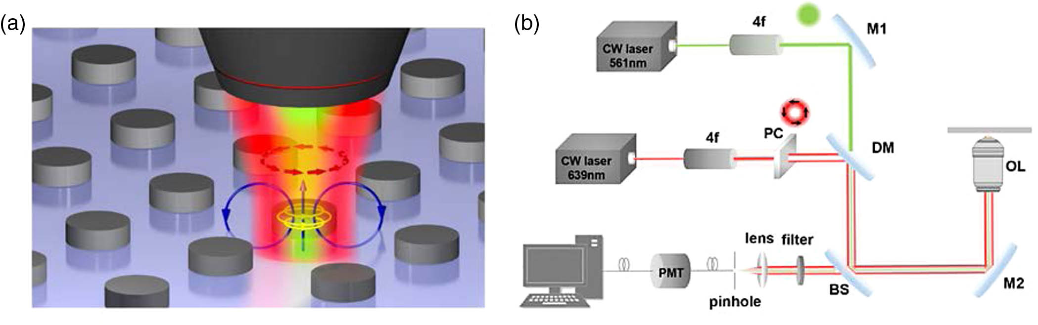
    Fig. 1. Schematic illustration of the superlocalization imaging and experimental setup. (a) The principle of superlocalization imaging is based on scattering suppression of Si nanodisks at the peripherals of the doughnut-shaped AP saturation beam. (b) Diagram of the reflectance laser scanning confocal system. M1, M2, silver mirrors; DM, dichroic mirror; BS, beam splitter; OL, objective lens; PC, polarization converter.
    Simulated total scattering spectra and the Cartesian multipolar decomposition of single Si nanodisks (diameter D=200 nm, height h=50 nm) under (a) linear and (b),(c) CVB illumination. Black dashed lines indicate the position of excitation wavelength.
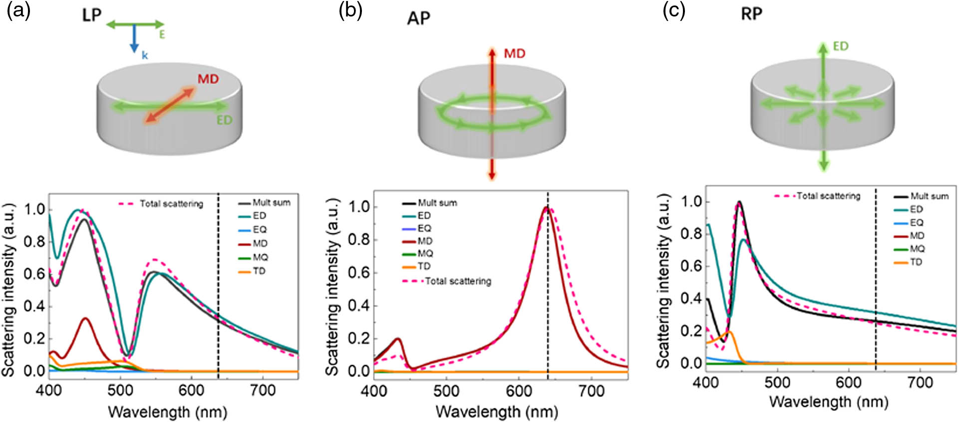
    Fig. 2. Simulated total scattering spectra and the Cartesian multipolar decomposition of single Si nanodisks (diameter D=200  nm, height h=50  nm) under (a) linear and (b),(c) CVB illumination. Black dashed lines indicate the position of excitation wavelength.
    Experimental observation of photothermal nonlinearity via backward scattering measurements using CVBs. (a)–(c) Measured PSFs of a single nanostructure under different AP beam intensities at a 639 nm wavelength. (a) At low excitation intensity, the PSF shows the doughnut-shaped focal spot generated from the conventional AP. (b),(c) When the intensity reaches a nonlinear region, scattering saturation occurs, and the corresponding PSFs show a low intensity at the doughnut crest. The intensity lateral profiles (white dashed lines) are plotted on the right. (d) The nonlinear dependency of scattering on irradiance intensities and the evolution of PSFs of the Si nanodisk array for AP excitations at a 639 nm wavelength; (e) for RP excitation, negligible nonlinearity is observed, and the scattering shows a linear response in accordance with the increasing irradiance intensities.
    Fig. 3. Experimental observation of photothermal nonlinearity via backward scattering measurements using CVBs. (a)–(c) Measured PSFs of a single nanostructure under different AP beam intensities at a 639 nm wavelength. (a) At low excitation intensity, the PSF shows the doughnut-shaped focal spot generated from the conventional AP. (b),(c) When the intensity reaches a nonlinear region, scattering saturation occurs, and the corresponding PSFs show a low intensity at the doughnut crest. The intensity lateral profiles (white dashed lines) are plotted on the right. (d) The nonlinear dependency of scattering on irradiance intensities and the evolution of PSFs of the Si nanodisk array for AP excitations at a 639 nm wavelength; (e) for RP excitation, negligible nonlinearity is observed, and the scattering shows a linear response in accordance with the increasing irradiance intensities.
    Superlocalization of densely spaced Si nanodisks. (a) PSFs of nonlinear scattering from periodic Si nanodisk arrays evolving with increasing excitation intensities. A correlated SEM image is also presented. (b) Localization accuracy scaling as PSFs obtained at different saturation AP beam intensities. The error bars represent the deviations of FWHM values from 28 nanodisks in the scanning frame. (c) Reversibility of nonlinear scattering is confirmed by the full recovery of measured FWHM from the same nanodisks under repetitive measurements.
    Fig. 4. Superlocalization of densely spaced Si nanodisks. (a) PSFs of nonlinear scattering from periodic Si nanodisk arrays evolving with increasing excitation intensities. A correlated SEM image is also presented. (b) Localization accuracy scaling as PSFs obtained at different saturation AP beam intensities. The error bars represent the deviations of FWHM values from 28 nanodisks in the scanning frame. (c) Reversibility of nonlinear scattering is confirmed by the full recovery of measured FWHM from the same nanodisks under repetitive measurements.
    SEM image and magnified image of Si nanodisk arrays with a diameter of 200 nm and height of 50 nm. Scale bar, 1 μm; 400 nm.
    Fig. 5. SEM image and magnified image of Si nanodisk arrays with a diameter of 200 nm and height of 50 nm. Scale bar, 1 μm; 400 nm.
    (a) AFM characterization of the Si nanodisk array sample. Scale bar, 400 nm. (b) Cross section of the height of the nanodisk at the position of the black dotted line.
    Fig. 6. (a) AFM characterization of the Si nanodisk array sample. Scale bar, 400 nm. (b) Cross section of the height of the nanodisk at the position of the black dotted line.
    Experimentally generated radial beam (upper row), azimuthal beam (lower row), and their linear orthogonal components. The black arrows indicate the position of the analyzer.
    Fig. 7. Experimentally generated radial beam (upper row), azimuthal beam (lower row), and their linear orthogonal components. The black arrows indicate the position of the analyzer.
    (a) Photothermal tuning of normalized scattering spectra of Si nanodisks of different polarization states at three representative temperatures: RT, 500°C, and 850°C. The dashed line indicates the position of excitation. (b) Evolution of Csca with increasing temperatures at the excitation wavelength of 639 nm; (c) required excitation intensities for temperature increase of the Si nanodisks under AP and RP illuminations; (d) resulting simulated nonlinear scattering behaviors under AP and RP illuminations; (e) simulated scattering cross sections for total scattering, forward scattering, and backscattering illuminated by AP excitation; (f) evolution of backscattering CscaB with increasing temperatures at the excitation wavelength of 639 nm.
    Fig. 8. (a) Photothermal tuning of normalized scattering spectra of Si nanodisks of different polarization states at three representative temperatures: RT, 500°C, and 850°C. The dashed line indicates the position of excitation. (b) Evolution of Csca with increasing temperatures at the excitation wavelength of 639 nm; (c) required excitation intensities for temperature increase of the Si nanodisks under AP and RP illuminations; (d) resulting simulated nonlinear scattering behaviors under AP and RP illuminations; (e) simulated scattering cross sections for total scattering, forward scattering, and backscattering illuminated by AP excitation; (f) evolution of backscattering CscaB with increasing temperatures at the excitation wavelength of 639 nm.
    Comparison of AP beam spot and doughnut-shaped circularly polarized beam spot. (a) The theoretic cross sections at the position of the white dashed lines in (b) are obtained with a laser of 639 nm. Scale bar, 400 nm. (c) The experimental cross sections at the location of the white dotted lines in (d) are obtained by scanning the Si with a diameter of 200 nm with a laser of 639 nm. Scale bar, 400 nm.
    Fig. 9. Comparison of AP beam spot and doughnut-shaped circularly polarized beam spot. (a) The theoretic cross sections at the position of the white dashed lines in (b) are obtained with a laser of 639 nm. Scale bar, 400 nm. (c) The experimental cross sections at the location of the white dotted lines in (d) are obtained by scanning the Si with a diameter of 200 nm with a laser of 639 nm. Scale bar, 400 nm.
    Bin Wang, Ying Che, Xiangchao Zhong, Wen Yan, Tianyue Zhang, Kai Chen, Yi Xu, Xiaoxuan Xu, Xiangping Li. Cylindrical vector beam revealing multipolar nonlinear scattering for superlocalization of silicon nanostructures[J]. Photonics Research, 2021, 9(6): 950
    Download Citation