
Song LIANG. InP Based Long Wavelength Transistor Lasers (Invited)[J]. Acta Photonica Sinica, 2020, 49(11): 116
- Acta Photonica Sinica
- Vol. 49, Issue 11, 116 (2020)
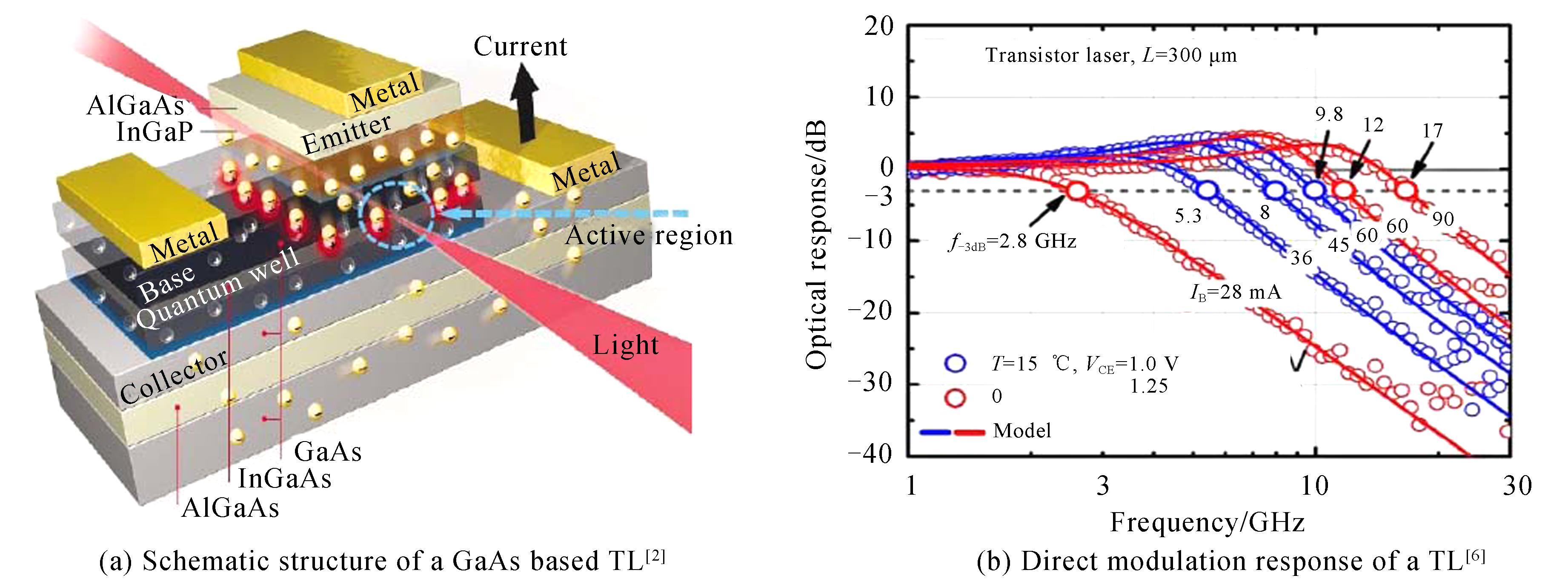
Fig. 1. Schematic structure and direct modulation response of a GaAs based TL
![Tunnel junction TL band and light power as a function of VCE[9]](/richHtml/gzxb/2020/49/11/116/img_2.png)
Fig. 3. Laser integrated with transistor by conventional and TL ways[11]
Fig. 4. Schematic structure and material structure of InP based shallow ridge TL[15]
Fig. 5. Light power as a function of base current of InP based shallow ridge TL[15]
Fig. 6. Schematic structure and common emitter mode opto-electronic properties of InP based buried ridge TL[18]
Fig. 7. Schematic structure of deep ridge TL and SEM cross-section picture of an InP deep ridge TL[21]
Fig. 8. Material structure of the room temperature deep ridge InP TL[24]
Fig. 9. Common emitter mode opto-electronic properties an InP deep ridge TL[24]
Fig. 10. Common emitter mode light power and current gain of TLs having doping level from 0 to 1×1018cm-3 in the MQWs
Fig. 11. Schematic structure and current distribution of a-TL[26]

Set citation alerts for the article
Please enter your email address
© Copyright 2018-2021 | Chinese Laser Press. All Rights Reserved 沪ICP备15018463号-20