We demonstrate a soft lithography approach for fabrication of a topographically patterned polyvinyl alcohol (PVA) liquid-crystal (LC) alignment layer. This specific approach employs modified micromolding in capillaries for negative replication of the PVA microstructures on indium tin oxide (ITO) substrates from patterned poly(dimethylsiloxane) molds in a single step, leading to planar alignment on the desired regions. By doping with polyhedral oligomeric silsesquioxane nanoparticles, which can induce vertical alignment on bare ITO surfaces, periodic LC phase gratings based on an alternating vertical-aligned/hybrid-aligned nematic geometry are presented as an application, and a theoretical model was used to simulate and examine the experimental results.
Recently, topological patterns with surface relief micro-structures have attracted intense attention due to their robust capability for precise manipulation of the focal conic domains (FCDs) in smectic liquid-crystal (LC) phases[1]. By controlling the dimensions and symmetry of the microstructures, the growth and arrangement of FCD defects can be directed. Many micro-fabrication techniques have been employed to fabricate these topological patterns. Quite a few of the most exciting works fall into an area known as soft lithography[2,3], which is inexpensive, convenient, and is of growing importance for a multitude of applications such as microfluidics, cell biology, lab-on-a-chip, and flexible electronics. Among them, micromolding in capillary (MIMIC) is remarkable for its fidelity in transferring the patterns from the mold to the polymeric structures by capillary filling the channels[4]. It can directionally constrain the growth of materials and pattern free-standing microstructures from a broad range of materials[5].
Soft lithography is such an appealing route that can also be used to pattern LC alignment layers, which are crucial to obtain LC devices with a periodic refractive index change[6,7]. Aside from rapid prototyping of both microscale and nanoscale structures, it can be used to yield patterned LC alignment layers of various materials and control the surface chemistry of them. Moreover, it is applicable to patterning the LC alignment layers with complex microstructures on curved or flexible substrates in a compelling way that cannot be addressed effectively with other sophisticated techniques, such as holographic recording[8], micro-rubbing[9], mask photopolymerization[10], and atomic force microscope (AFM) patterning[11].
For example, soft imprint lithography is used for exact duplication of rubbed polyimide substrates to form alignment layers[12]. It can also produce polymer films with checkerboard patterns of square wells, which vertically align rod-shaped LCs in both nematic and smectic phases[13]. Using microcontact printing method, Chae et al. formed durable, ultrathin LC alignment layers that ensure a fast response time, thermal stability, and compartmentalized multidomain alignment[14]. It was also demonstrated that replica molding was employed to fabricate a flexible LC device[15]. In this Letter, we propose a modified MIMIC approach for the fabrication of a topography patterned LC alignment layer using polyvinyl alcohol (PVA). To illustrate the present method, several PVA gratings with different periods were fabricated. Combining rubbing PVA stripes with nanoparticle-induced vertical alignment, which was previously implemented by doping polyhedral oligomeric silsesquioxane (POSS) into LCs[16], we obtained LC phase gratings based on an alternating vertical-aligned (VA)/hybrid-aligned nematic (HAN) geometry. The fabrication process and the characterization of the LC cells are described, and the experimental results are analyzed using a model of the LC phase grating.
Sign up for Chinese Optics Letters TOC. Get the latest issue of Chinese Optics Letters delivered right to you!Sign up now
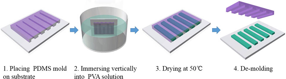
The poly(dimethylsiloxane) (PDMS) elastomeric mold was prepared by cast molding. First, the prepolymer of PDMS, a mixture of the elastomer base and curing agent (Dow Corning, Sylgard 184) at a weight ratio of , was poured over the silicon master with different topographic patterns. It was necessary to place the mixture under a laboratory vacuum for 10 min to remove the air bubbles from the mixture. Subsequently, the mixture was cured at 60°C for over 6 h and peeled off.
Using the fabricated PDMS mold, we patterned the alignment layer on cleaned indium tin oxide (ITO) glass by modified MIMIC as depicted in Fig. 1. We cut redundant PDMS off and opened both ends of the channels. After that, the PDMS mold was rinsed several times and blown dry with clean nitrogen. The PDMS mold was placed on the surface of the cleaned ITO glass and the conformal contact between them formed a network of empty channels. Then, they were vertically placed into a 5 wt. % PVA (molecular weight , alcoholysis degree 87%–89%, Aladdin Reagent Co., China) solution such that one open end of the capillary was immersed below the liquid level while the other was above the liquid level. After the PVA solution eventually filled the channels by capillary action, they were baked at 50°C. When the solvent was removed by evaporation, the PDMS mold was peeled off, and the solidified PVA confined within the channels formed patterned microstructures on the surface of the ITO glass. Surface profiles of the patterned PVA structures was studied using a scanning electron microscope (SEM; HITACHI S4800) and an AFM (Veeco 3D). Afterwards, we mechanically rubbed the substrate with patterned PVA structures to achieve planar alignment; the rubbing direction was parallel to the PVA stripes.
Figure 1.Fabrication process of patterned PVA structures.
An empty cell, separated by 9 μm spacers, was then fabricated using an ITO glass substrate with rubbed PVA microstructures on its surface and an ITO glass substrate without any treatment. The aminoethyl aminopropylisobutyl POSS (Aldrich) nanoparticles were dissolved in the positive dielectric anisotropic LC (E7, Xianhua Chemical Co. China) at a weight ratio of 0.5% through acetone solvent and mixed in an ultrasonic bath. After thorough mixing, the mixture was baked in a vacuum oven at 60°C for 5 h to evaporate residual acetone. Finally, the mixture was injected into the empty LC cells using capillary action.
Multiple copies of the PDMS mold can be easily fabricated from a single silicon master, and they can be reused many times. The PDMS mold used in our work has stripe-type relief structures on its surface, and the grating periods () are about 11.7, 13.6, 15.6, and 17.3 μm. Figures 2(a) and 2(b) present the images of a LC cell under ambient light and between cross polarizers. Figures 2(c)–2(f) show SEM images of the fabricated PVA relief structures on ITO glass by modified MIMIC. The AFM image of the sample in Fig. 2(e) is shown in Fig. 2(g).
Figure 2.(a) and (b) Photographs of LC cell under ambient light and between cross polarizers; (c)–(f) SEM images of the fabricated PVA relief structures with periods of 11.7, 13.6, 15.6, and 17.3 μm, respectively; (g) AFM image of the sample with a period of 15.6 μm; (h) depth profile of the PVA relief structures highlighted by the dotted line in Fig. 2(g).
The images confirmed that the overall structures of the surface relief on PDMS are successfully replicated by the patterned PVA layer in this range of length scale. Figure 2(h) depicts the depth profile of the PVA relief structures highlighted by the dotted line in Fig. 2(g). The cross section indicates that the structures obtained from this approach are thinner than the height of the channels in the PDMS mold and both sides of them lean towards the center. The height of the sample in Fig. 2(e) is about 619 nm. In this context, we defined the width of PVA stripe () as the top width value of the structure. Consequently, the duty cycle (; the ratio of to ) is calculated to be about 0.334. Pattern replication by capillary-driven flow significantly reduces the extent of stresses accumulated within replicated structures, enhancing the long-term durability. Although there are some shrinkage problems associated with evaporation of the solvent, the resulting structures have approximately the same lateral dimensions. PVA is easily accessible in conventional laboratories such that the method established in our work can be readily extended to fabricate more-complex PVA alignment patterns.
Periodic VA/HAN LC phase gratings were demonstrated as an application by assembling a LC cell with one ITO glass substrate with rubbed PVA stripe-type microstructures on its surface and the other without any treatment. The chemical structure of the POSS molecule used in our experimental work is shown in Fig. 3(a), with indicating the functional group. After adding POSS in LC, the POSS in the LC cell can induce vertical alignment of the LC on their functional group as per Sharp’s concept[17]. As the concentration of POSS doped in E7 is important for LC alignment, LC cells with various POSS concentrations were observed under a cross polarizer polarizing optical microscope (POM), as shown in Figs. 3(b)–3(e). The POM images indicate that a low POSS concentration cannot induce a good vertical alignment, and will lead to the light leakage. Conversely, a high POSS concentration may cause nanoparticles to aggregate, form clusters, and induce severe light scattering loss. Consequently, we choose 0.5 wt. % as the optimum concentration of POSS dopant.
Figure 3.(a) Structure of POSS molecule used in our experimental work; (b)–(e) polarizing microscope images of LC cells doped with 0.2, 0.5, 0.6, and 0.8 wt. % POSS, respectively. All the LC cells have the same cell gap .
The microscopic textures of the LC phase gratings, observed under a cross polarizer POM, when the rubbing direction makes angles of 0° and 45° with respect to the analyzer are presented in Fig. 4. The POM image of the hybrid aligned regions changes from dark to bright due to the combined effect of the rubbed PVA layer and POSS, while the regions of vertically alignment produced by POSS remain dark when the angle between the rubbing direction and the analyzer is changed from 0° to 45°. We also observed that the LC grating exhibited, to some extent, a grating effect in the absence of an applied voltage, although an ideal LC phase grating should not have this effect. This phenomenon is induced by the initial curvature distortions of the LC at adjacent region boundaries in the periodically alternating VA/HAN geometry[18]. The proposed VA/HAN geometry of the LC phase gratings was verified and is depicted in Fig. 4(c). Basically, LC molecules are vertically aligned in the regions where bare ITO surfaces are face-to-face, and hybrid aligned in the regions where one substrate is coated with rubbed PVA stripes and the opposite is a bare ITO surface.
Figure 4.(a) and (b) Images of the 15.6 μm LC phase grating observed under a cross polarizer POM when the angles between the rubbing direction and the analyzer are 0° and 45°, respectively; (c) schematic diagram of LC phase gratings based on an alternating VA/HAN geometry.
Figure 5 plots the measured first-order diffraction efficiency of LC phase grating () as a function of the applied AC (1 kHz) voltage for a fixed input wavelength of 635 nm. It should be noted that the probed beam with its polarization along the -direction (perpendicular to the rubbing direction) is quite insensitive to the applied voltage, whereas the probed beam polarized along the -direction (parallel to the rubbing direction) shows a strong dependence on the voltage. The first-order diffraction efficiency has the maximum, 28.4%, when the applied voltage is about 1.5 V.
Figure 5.First-order diffraction efficiency of the 15.6 μm LC phase grating as a function of the applied AC (1 kHz) voltage for a fixed input wavelength of 635 nm. Red and black open symbols, experimental data probed using a polarized laser beam with its polarization parallel and perpendicular to the rubbing direction, respectively. Inset A, diffraction pattern of LC phase grating. Inset B, measured response time of the first order.
Figure 5, Inset A, shows the diffraction pattern of the LC phase grating; Fig. 5, Inset B, shows the response time for the first-order diffraction under 1.5 V, where the maximum efficiency occurs. The rise time and decay time are defined as 10%–90% of the transmittance change. We find that the rise time is 50.2 ms and the decay time is 187 ms. The detailed characteristics of the LC phase gratings with different periods, including the measured grating parameters of PVA relief structures, the maximum diffraction efficiency that we can achieve, and so on, are summarized in Table 1. Table 1 shows that the height of the PVA strips with different periods ranges from 550 to 700 nm, and the diffraction maximum is related to the duty cycle. The rise time of gratings with different periods are almost the same, whereas the decay time increases as the period increases.
PVA Relief Structure
First-Order Diffraction Efficiency
Λ (μm)
Height (nm)
Duty Cycle D
Maximum (%)
Rise Time (ms)
Decay Time (ms)
11.7
685
0.298
26.1
49.8
166
13.6
578
0.328
27.4
50.4
173
15.6
619
0.334
28.4
50.2
187
17.3
555
0.319
27.2
49.2
358
Table 1. Characteristics of the LC Phase Gratings with Different Periods
We analyze the voltage responsive first-order diffraction efficiency of VA/HAN-type LC phase gratings in the following. In view of that the rubbing direction is along the -direction as shown in Fig. 4(c), the probed beam polarized along the -direction will not experience any relative phase difference after passing through two adjacent regions. Nevertheless, the probed beam polarized along the -direction will exhibit relative phase retardation only through the hybrid aligned region. The relative phase difference between two adjacent vertical and hybrid regions can be given as[19]where is the cell gap, is the wavelength of the probed beam, and is the effective refractive index at in the hybrid aligned region, which is determined by[19]where and are the extraordinary and ordinary refractive indices, respectively, of the LC mixture; is the tilt angle at in the hybrid aligned region.
In order to obtain , the distribution of the LC directors is calculated using a numerical method based on the finite-difference approximation to the Euler–Lagrange equation[20]. We consider a one-dimensional model and assume that the surface free energy can be ignored in the strong anchoring case. We choose the following parameters in the simulations: , , , , , , , and . By using the director profile when the applied voltage is zero as the initial profile, the deformation profiles of the hybrid aligned region are calculated. Accordingly, the under a given applied voltage can be calculated by substituting into Eq. (2). and ε⊥ are the dielectric permittivities of the material parallel and perpendicular to the director, respectively. ε⊥. K11, K22, and K33 are the splay elastic constant, twist elastic constant, and bend elastic constant, respectively.
For the LC phase gratings, the diffraction efficiency of the first order is then obtained as follows[21]
Substituting the duty cycle of LC phase gratings into Eq. (3), we can evaluate the theoretical as a function of the applied AC voltage. In this context, we adopted the measured parameters of the typical LC phase grating (). It is known that the pretilt angle of LC molecules on a planar aligned surface can be influenced by the doping of different concentrations of POSS nanoparticles; we assumed the value of the LC pretilt angle on rubbed PVA stripes is 18°[22].
As shown in Fig. 6, the maximum of the theoretical first-order diffraction efficiency is 30.5% [ in Eq. (3)] and the applied AC voltage corresponding to the maximum is about 1.5 V, which coincides well with the experimental result. There is a difference between the theoretical and experimental result in the low-voltage limit due to the initial curvature distortions of the LC at adjacent region boundaries, which has been discussed in Fig. 4. The difference in shape between the theoretical curve and experimental result may come from the change in the dielectric constant, which is induced by the doping POSS nanoparticles.
Figure 6.Experimental and theoretical first-order diffraction efficiencies of the 15.6 μm LC phase grating as a function of the applied AC voltage. Red symbols, experimental result; blue symbols, theoretical prediction.
In conclusion, we demonstrate the feasibility of fabricating a topologically patterned PVA alignment layer by our modified MIMIC method and its utilization in LC phase gratings. The proposed approach opens a route to fabricating a PVA alignment layer selectively only onto the desired regions of the substrate in a single step. The fabricated PVA layers can also guide material deposition on or removal from the substrate to yield patterns of other materials. VA/HAN-type LC phase gratings with different periods of 11.7, 13.6, 15.6, and 17.3 μm are obtained by doping with POSS nanoparticles, which can induce vertical alignment on the ITO surface. Their voltage-responsive diffraction behaviors are investigated. A first-order diffraction efficiency of up to 28.4% is recorded and coincided well with the theoretical value of 30.5%, which reveals the consistency of the proposed VA/HAN model.
[14] S. S. Chae, H. Min, J. H. Lee, B. Hwang, W. M. Sung, W. S. Jang, Y. B. Yoo, J. Y. Oh, J. H. Park, D. Kang, D. Kim, Y. S. Kim, H. K. Baik. Adv. Mater., 25, 1408(2013).