
Ting Hu, Bowei Dong, Xianshu Luo, Tsung-Yang Liow, Junfeng Song, Chengkuo Lee, Guo-Qiang Lo, "Silicon photonic platforms for mid-infrared applications [Invited]," Photonics Res. 5, 417 (2017)
- Photonics Research
- Vol. 5, Issue 5, 417 (2017)
![Material absorption characteristic in the MIR range [1,3]. Gray region represents the optical transparency; black area denotes the high loss. Absorption peaks of some detected gases and the fingerprint region are marked.](/richHtml/prj/2017/5/5/05000417/img_001.jpg)
Fig. 1. Material absorption characteristic in the MIR range [1,3]. Gray region represents the optical transparency; black area denotes the high loss. Absorption peaks of some detected gases and the fingerprint region are marked.
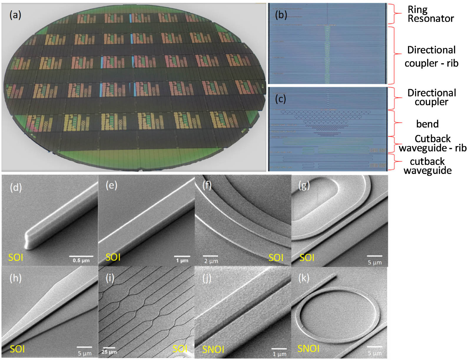
Fig. 2. (a) Fabricated 8-in. silicon wafer with MIR devices after wafer dicing for characterization. (b) SOI strip ring resonators and rib DCs. (c) SOI strip DCs, bends, waveguides, and rib waveguides. (d)–(k) SEM images of the fabricated devices. (d) SOI waveguide taper tip. (e) SOI strip waveguide. (f) SOI rib waveguide. (g) SOI rib DC. (h) SOI strip to rib converter. (i) SOI strip DC array. (j) SNOI DC. (k) SNOI add–drop ring resonator.
Fig. 3. Loss characterization of SOI waveguide. (a) Propagation loss of SOI strip waveguide. (b) Bending loss of SOI strip waveguide. (c) Propagation loss of SOI rib waveguide. Insets in (a) and (c) show the corresponding mode field simulated by the commercial software Lumerical FDTD.
Fig. 4. Characterization of SOI strip and rib DCs. (a) and (c) Self-normalized transmitted and coupled power of (a) strip and (c) rib DCs. Solid lines show sine squared fitting of the data with adjusted R-square of 0.997. (b) and (d) Power coupling coefficient K L c L π Ø 0
Fig. 5. Characterization of SOI strip racetrack resonators. Red dots present measurement data, while the blue solid lines show fitting results. (a) and (c) Transmission spectra of the racetrack resonator with (a) r = 5 μm g = 500 nm L c = 50 μm r = 5 μm g = 550 nm L c = 10 μm ∼ 3687 nm ∼ 3824 nm
Fig. 6. Loss characterization of SNOI waveguide. (a) Propagation loss of SNOI strip waveguide. (b) Bending loss of SNOI strip waveguide. Inset in (a) shows the mode field simulated by Lumerical.
Fig. 7. Characterization of the SNOI strip ring resonator with radius of 20 μm and coupling gap of 550 nm. Transmission spectrum of the ring resonator (a) from 1960 to 2045 nm with scanning step of 0.54 nm (b) around the resonance of 1988 nm with scanning step of 0.011 nm.
Fig. 8. CO 2 CO 2 Q CO 2
|
Table 1. Demonstrated MIR Waveguides with Various Platforms
|
Table 2. Demonstrated MIR MRRs with Various Platforms


Set citation alerts for the article
Please enter your email address

© Copyright 2018-2021 | Chinese Laser Press. All Rights Reserved 沪ICP备15018463号-20