1Huazhong University of Science and Technology, School of Optical and Electronic Information, Wuhan National Laboratory for Optoelectronics, Wuhan, China
2The Chinese University of Hong Kong, School of Science and Engineering, Shenzhen, China
3CAS Center for Excellence in Nanoscience, National Center for Nanoscience and Technology of China, Nanofabrication Laboratory, CAS Key Laboratory for Nanosystems and Hierarchical Fabrication, CAS Key Laboratory for Nanophotonic Materials and Devices, Beijing, China
4National University of Singapore, Department of Electrical and Computer Engineering, Singapore
5University of Chinese Academy of Sciences, Center of Materials Science and Optoelectronics Engineering, Beijing, China
6The University of Hong Kong, Department of Physics, Hong Kong, China
7Peking University, School of Physics, State Key Laboratory for Mesoscopic Physics, Beijing, China
Topological edge states (TESs), arising from topologically nontrivial phases, provide a powerful toolkit for the architecture design of photonic integrated circuits, since they are highly robust and strongly localized at the boundaries of topological insulators. It is highly desirable to be able to control TES transport in photonic implementations. Enhancing the coupling between the TESs in a finite-size optical lattice is capable of exchanging light energy between the boundaries of a topological lattice, hence facilitating the flexible control of TES transport. However, existing strategies have paid little attention to enhancing the coupling effects between the TESs through the finite-size effect. Here, we establish a bridge linking the interaction between the TESs in a finite-size optical lattice using the Landau–Zener model so as to provide an alternative way to modulate/control the transport of topological modes. We experimentally demonstrate an edge-to-edge topological transport with high efficiency at telecommunication wavelengths in silicon waveguide lattices. Our results may power up various potential applications for integrated topological photonics.
Topological insulators exhibit many intriguing effects and phenomena in various physical disciplines,1–4 including electronics, acoustics, and photonics. Topological edge states (TESs), protected by topologically nontrivial phases, have captured wide attention due to their robustness against disorders and imperfections. TES transport has led to many exotic optical effects and applications, such as robust directional couplers,5 one-way waveguides,6 mode-locked waveguides,7 and pseudospin propagation in ring resonator arrays,8 which are of fundamental importance for groundbreaking technologies. TESs are promising for developing energy and information routers in nanophotonic circuits, benefiting from their robust transport and strong localization at the boundaries of topological insulators. Recent works have expanded the research on manipulating TESs, including the adiabatic modulation,9–11 the nonlinear effect,12 and the complicated braiding.13 A variety of intriguing physical phenomena have been demonstrated in optical systems, such as the edge-to-edge topological transport,5,10,14–16 the topological states with tunable localization,17,18 the higher-order topological protection,19,20 the nonlinear excitation of topological modes,21,22 and the non-Abelian process.23,24 These unique phenomena may facilitate the development of many important technologies and applications, including routing energy and information,25 quantized transport,9 nonlinear photonics,26 and quantum computing.27 Though these phenomena have been extensively studied in photonic systems, little work has been focusing on enhancing the coupling effects between TESs under the topological protection through the finite-size effect. Enhancing the interaction between the TESs may provide a way of exchanging light energy between the boundaries of topological lattices, beneficial to the flexible control of TES transport.
The Landau–Zener (LZ) model, initially established to study the dynamics in a two-level quantum system,28,29 can be employed to predict the probability of nonadiabatic tunneling between two energy levels.30,31 This model has been widely applied to investigate the tunneling effect in condensed matter physics,32,33 multi-particle systems,34,35 optical structures,36–38 and acoustics.39 The LZ model provides an easy yet effective way to modulate/control the light transport due to its flexible and convenient realization in 2D optical circuits. More recently, researchers have combined the LZ model and the nonparaxiality model to achieve spoof surface plasmon channel conversion in the microwave region.38 However, the previous studies on the LZ model in optical systems were merely focused on its tunneling effects, such as LZ Bloch oscillations36 and Rabi oscillations,37 while its counterpart, the LZ single-band evolution process in optical systems, has been rarely studied to date.
In this paper, we report edge-to-edge channel conversion in a four-level waveguide lattice with the LZ model. We show that it is able to link up the coupling between TESs by the finite-size effect in a two-unit-cell optical lattice to provide an alternative, effective, and dynamic paradigm to modulate/control the transport of topological modes. The waveguide lattice corresponds to an interval of an entire modulation period. The underlying mechanism of such a waveguide lattice is equivalent to a 2D Chern insulator, and the existence of TESs is predicted. The TESs are dynamically controlled with the LZ single-band evolution principle, and a near-unity-efficiency edge-to-edge channel conversion is experimentally demonstrated in the silicon photonic platform at 1550 nm.
Sign up for Advanced Photonics TOC. Get the latest issue of Advanced Photonics delivered right to you!Sign up now
2 Results and Discussion
2.1 Landau–Zener Model in Harper Waveguide Lattices
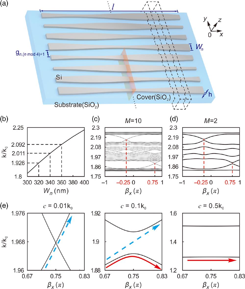
A silicon optical waveguide lattice with the presence of nearest-neighbor coupling is shown in Fig. 1(a), and it is constructed to demonstrate the four-level Harper model.40 The bulk Hamiltonian of the waveguide lattice is where the number sets and denote the external and internal degrees of freedom, respectively. In this case, labels the states on the th waveguide in the th unit cell, and is the number of unit cells. The hopping strength corresponds to the coupling coefficient whose estimation can be found in Sec. 1 in the Supplementary Material and is the propagation constant of the fundamental mode in the th waveguide [Fig. 1(b)]. The waveguide lattice can be regarded as a four-level Harper model, if the waveguide propagation constant is modulated as , with the coupling coefficient equal to a constant , where is the coupling coefficient in Harper model. For the specific configuration studied, we set , , and . The corresponding geometric parameters of the designed waveguide lattice will be provided in detail in the following section. It should be noted that the practical waveguide widths are varied along the propagation direction. As a result, the coupling coefficients are thus slightly different from the values used in the above model. Figure 1(c) shows the propagation constant spectral flow of the four-level Harper model with . The bands are degenerated at the crossing points and . The finite-size effect requires employing a limited number of unit cells . A minimum is found more suitable to open the gap [Fig. 1(d)]. Interestingly, how the finite-size effect affects the energy bandgap has been studied in the platform of condensed matter physics, and the coupling strength can be characterized by the Berry connection.41
Figure 1.LZ model in Harper waveguide lattices. (a) Conceptual map of silicon optical waveguide lattice with unit cells for demonstrating four-level Harper model. The width of the th waveguide is , determining the propagation constant of the fundamental TE waveguide mode, and each waveguide has a height of , and length of corresponding to the modulation period. The is the separation distance between the th and th waveguides, which is closely related to the coupling coefficient . (b) Propagation constant of fundamental TE mode versus . The propagation constant spectral flow of Harper model with (c) and (d) , where is the evolution parameter normalized to along the propagation direction. (e) LZ model near with different coupling coefficients . All the propagation constant spectra are normalized to the free space wavenumber of light, ().
To analyze the evolution of the states around minimum bandgap points, a widely used method is to characterize the band with an approximate two-level model, i.e., the LZ model,31,39
Here is the slope of the band near minimum bandgap points, and is the minimum gap size. This model corresponds to a certain modulation interval within an entire period. In the following, we will study the evolution of the state near .
As the coupling strength is very small, the band is gapless [see the left panel of Fig. 1(e) with ]. The model supports LZ tunneling process only, represented by the dashed blue line in Fig. 1(e), and the state can hop to the nearest band. As the coupling strength is increased to [see the middle panel of Fig. 1(e)], both of the LZ tunneling and single-band evolution contribute to the state evolution. The LZ single-band evolution, represented by the solid red line in Fig. 1(e), occurs in the same band.
We have calculated the probability of LZ tunneling and LZ single-band evolution (Sec. 2 in the Supplementary Material). The parameter is projected over the propagation distance with , and the equal-probability distance is , at which the LZ tunneling and LZ single-band evolution share equal probability. is the length of the modulation period, affecting the evolution speed. It is worth noticing that a recent study on topological pumps has shown that the evolution speed will influence the final states after traveling an entire cycle.42 With a definition of the evolution speed as ( is the actual device length affecting the evolution speed), the tunneling probability is enhanced, associated with weakened adiabaticity (see more details in Sec. 2 in the Supplementary Material). It should be mentioned that the equal-probability distance is not equivalent to the adiabatic limit in quantum mechanics and condensed matter physics.42 The adiabatic approximation condition can be guaranteed with . As the coupling strength is sharply increased to [see the right panel of Fig. 1(e)], the bands are flat near , allowing LZ single-band evolution. However, it is hard to obtain such strong coupling strength in coupled waveguides. For the waveguide lattice [Fig. 1(a)], the nearest-neighbor coupling coefficient between waveguides approaches as is close to zero, associated with the upper limit of the energy gap of .
2.2 Dynamic Manipulation of Topological Edge States
To demonstrate the LZ single-band evolution, we have designed practical silicon waveguide lattices [Fig. 2(a)] with the spectral flow near , as shown by the middle panel of Fig. 1(e). Different from a topological pump on the three-level Harper model where periodical modulation potential is required,9,10 our waveguide lattice is described by the four-level Harper model, corresponding to an interval within an entire modulation period, associated with the region bounded by the dashed black frame in Fig. 1(a). In contrast to a topological pump that has gapless spectrum flow, we have used the finite-size effect to open the spectrum flow, which enables us to manipulate TESs through the LZ single-band evolution. For practical experimental implementation, we have employed a linear variation of waveguide widths (see the detailed structural parameters in Sec. 3 in the Supplementary Material), instead of the variation described by a cosine function, as in Fig. 1(a). We first focus on the three cross sections at , , and , and each cross section can be regarded as a 1D four-level near-neighbor hopping chain with bulk momentum-space Hamiltonian,43where ( and ), , ( and ), , ( and ), , , and ( and ) in the cross section at ( and ). By solving the eigenstates of the Hamiltonian, the Zak phase of four bands can be calculated as (see more details in Sec. 4 in the Supplementary Material). Figure 2(b) shows the Zak phases at three different cross sections, indicating that both the first and second bands support nonzero Zak phases corresponding to nontrivial topological phases. The Zak phases of the other two bands are close to zero, corresponding to a trivial topological phase. According to the bulk-boundary correspondence,43 there exist two TESs in the first bandgap. As shown in Fig. 2(c), the two TESs are chiral at the cross sections when and , while their field intensities are symmetrical when .
Figure 2.Topological phase and edge states of the Harper waveguide lattice. (a) Silicon eight-waveguide lattice with length , near . This structure refers to the region bounded by the dashed black frame in Fig. 1(a). (b) The Zak phase of 1D finite chain model corresponding to three different cross sections with , , and . The red and blue dots represent the Zak phase of the first band and fourth band, respectively. The orange and purple rhombus denote the Zak phase of the second band and third band, respectively. (c) The cross-sectional field intensity distributions of with , , and . The upper (lower) three figures correspond to TES1 (TES2). (d) The Bloch bands of the waveguide lattice shown in Fig. 1(a) in 2D parameter space under periodical boundary condition. is the Bloch vector in the reciprocal space along the direction. The Chern numbers of four bands are labeled by the white characters.
The above theoretical analysis on TES is limited to 1D insulators and does not involve dynamic modulation during propagation. Through Fourier transformation and by solving for eigenvalues of the bulk momentum-space Hamiltonian associated with the Harper waveguide lattices in Fig. 1(a), the eigenvalue spectrum in the 2D parameter space is presented in Fig. 2(d) (see more details in Sec. 5 in the Supplementary Material). The Chern numbers of the bands are calculated using the Wilson loop method (see more details in Sec. 4 in the Supplementary Material). It should be emphasized that the coupling coefficients used in the Harper waveguide lattice in Fig. 1(a) are slightly different from those used in the actual linear waveguide lattice in Fig. 2(a). However, the difference in coupling coefficients is negligible and hence will not change the nontrivial topological phase. Thus, the TESs are protected by the nonzero Chern numbers within the entire modulation interval. If the adiabatic limit is satisfied (), the associated TESs will follow the LZ single-band evolution, and the optical field will be transferred from one boundary across the bulk waveguides to another side, i.e., adiabatic edge-to-edge channel conversion. If is below , the TESs will tunnel and the optical field will stay at one boundary.
2.3 Simulation and Experimental Demonstration
Numerical simulations by finite-difference time-domain are conducted to verify the LZ dynamics between two TESs. The two TESs are the second and third eigenmodes in the eight-waveguide lattice, and the field intensity is mainly located in the eighth and first waveguides, respectively. We have adjusted the waveguide lengths to illustrate how the degree of adiabaticity affects LZ dynamics. When is below the equal-probability distance , the tunneling process dominates and mode 3 (mode 2) converts to mode 2 (mode 3) in the upper (lower) panel of Fig. 3(a). To quantitively evaluate the percent of optical energy involved in LZ single-band evolution, we have defined the conversion efficiency as the energy ratio of the residual input mode at the output side to the total input mode. There is optical energy tunneled to another mode at with (see more simulated details in Sec. 6 in the Supplementary Material). When is approaching , the tunneling probability is [Fig. 3(b)]. Mode 2 (mode 3) is excited when mode 3 (mode 2) is injected from the left side. The excited mode and the injected mode undergo interference during propagation. As a result, the field energy is transferred between the first and eighth waveguides during propagation, and the ratio of their energies depends on the propagation distance. The percentage of tunneling to another mode reduces to 44%, while the percentage of adiabaticity is enhanced to 56%, as compared with . When is further increased and exceeds , the LZ single-band evolution dominates and tunneling effect is suppressed, accompanied by edge-to-edge channel conversion with high efficiency [Fig. 3(c)]. The estimated conversion efficiencies of the two TESs all exceed 93% around with and (see more simulated details in Sec. 6 in the Supplementary Material).
Figure 3.Edge-to-edge channel converter with different device lengths. The field intensity distributions of for edge-to-edge channel conversion of the two TESs in the waveguide lattice in Fig. 2(a). (a) , (b) , and (c) .
The edge-to-edge channel conversion with silicon waveguide lattices is experimentally demonstrated. Figure 4(a) shows the scanning electron microscope (SEM) image of the fabricated devices. More fabrication process, structural parameters, and SEM details for sections A, B, and E can be found in Sec. 7 in the Supplementary Material. The amplified SEM image for the waveguide lattice in section C is presented in Fig. 4(b). A tapered waveguide array with length is connected to waveguides 2–6 [Fig. 4(c)]. The width of each waveguide shrinks quickly to zero, and hence the bulk energy will be leaky. The resultant optical field energy of TESs is mainly localized at the boundary waveguides (waveguide 1 or waveguide 8), as indicated by the simulation results in Figs. 4(d) and 4(e). The localized optical energy in waveguides 1 and 8 finally outputs through ports 2 and 3, respectively, through two bending waveguides with a bend radius of and a straight waveguide, as shown by section D in Fig. 4(a).
Figure 4.Experimental demonstration. (a) SEM image of the device. The upper (lower) panel is used to test the edge-to-edge channel conversion effect of TES2 (TES1) with . Sections A and E are the grating couplers for coupling in and out of the waveguide energy, respectively. Section B corresponds to the adiabatic coupler for exciting the TESs, and section D represents output branch waveguides for testing the conversion effect. (b) The partially amplified SEM image for section C associated with Fig. 2(a). (c) The amplified SEM image for the region bounded by the dashed-line rectangle in section D. The simulated field intensity distributions of with TES2 (d) and TES1 (e). The simulated and experimental power contrast ratio , versus light wavelength with (f) and (g) . The red circles (lines) and blue circles (lines) represent the estimated and from the experiment (simulation), respectively.
The edge-to-edge channel conversion performance of the two TESs was evaluated by use of power contrast ratio and , with [see the upper panel in Fig. 4(a)] and [see the lower panel in Fig. 4(a)]. The optical power at port 2 and port 3, marked as and , respectively, is estimated by detecting the optical power with a spectrometer (see Sec. 7.3 in the Supplementary Material for the details of the measurement scheme). Figures 4(f) and 4(g) show the power contrast ratio of the output light with input from mode 2 (mode 3). Either or maintains a high value around . It clearly indicates the optical field is transferred from one side to the other with high efficiency. The experimental results show some deviation from simulations, which can be attributed to the fabrication error arising from etching roughness precision and the residual smudges during the fabrication process.
In nanophotonic circuits, waveguide couplers, such as directional/adiabatic couplers,44,45 are key components for routing energy and information. The practical device performance is highly sensitive to the cross-sectional geometry. The topological channel converter based on the LZ single-band evolution shows stronger cross-sectional tolerance, in contrast to these conventional couplers. We have theoretically analyzed the robustness against parameter perturbation by changing the gap separation given in Fig. 1(a). The topological phase transition point is calculated as the distances are varied. The theoretical results indicate the device shows certain robustness against all the gap distances (see more theoretical analysis in Sec. 8.1 in the Supplementary Material). As an example, the experimental results demonstrate that the gap distance can tolerate the perturbation up to (see the experimental validation in Sec. 8.2 in the Supplementary Material). The structural parameters along the direction are experimentally determined by electron-beam lithography (EBL), whose pattern resolution is much lower than the degree of tolerance for the sample. As for the direction, the etching error arising from inductively coupled plasma (ICP) is typically below 10 nm. We can therefore ignore the fabrication error along this direction. In addition, we study how the level number affects the topological phase transition point and find that the topological phase transition point approaches zero as grows. Although we have only theoretically and experimentally studied a four-level system in our work, a system based on a higher-level Harper model promises even stronger robustness (see more details in Sec. 9 in the Supplementary Material). The presented topological LZ nanophotonic devices can be extended to study other optical fields in nanophotonics. For example, they can serve as wavelength-dependent switches by tuning the operating wavelength to govern whether or not the field jumps between edges, when the device length is less than or comparable to (see the detailed discussions in Sec. 6 in the Supplementary Material). Introducing LZ dynamics into non-Hermitian systems may enable chiral channel conversion.46,47 The scheme may be further extended to non-Abelian adiabatic process on planar nanophotonic integration circuits with the proper design of waveguide lattices supporting higher-order degenerate eigenmodes.23,24
3 Conclusion
We have proposed LZ dynamics to dynamically manipulate the transport of topological states at optical frequencies. By constructing waveguide lattices with a finite size, LZ tunneling is suppressed. A high-efficiency edge-to-edge channel converter is theoretically designed based on LZ single-band evolution and experimentally verified at telecommunication wavelengths on a silicon platform. The topological LZ optical devices exhibit certain robustness to structural parameters. Theseresults provide an avenue to developing topological LZ nanophotonic devices and empower new opportunities for practical devices and applications. In the meantime, the edge-to-edge channel converter can function as a binary optical switching function unit in optical routing networks on chip.48 We can also use multiple cascaded edge-to-edge channel converters to serve as a multiplexer or demultiplexer through coupling or decoupling multiple channel signals into or out of a bus waveguide.49–55
4 Appendix: Materials and Methods
4.1 Fabrications
The fabrication of the devices is combined with three-step EBL, ICP etching, electron-beam evaporation (EBE), and plasma-enhanced chemical vapor deposition (PECVD). The first-step EBL and EBE aim to form the Au marks on a silicon-on-insulator wafer for alignment. The second-step EBL and ICP are used to define the grating couplers [sections A and E in Fig. 4(a)]. The adiabatic coupler, silicon waveguide lattices, and output branch waveguides [section B, C, and D in Fig. 4(a)] are fabricated by the third-step EBL and ICP. Finally, PECVD is applied to deposit a -thick cladding layer to cover the entire device. More details on structural parameters and fabrication are given in Secs. 3 and 7 in the Supplementary Material.
4.2 Measurements
The near-infrared light is provided by an amplified spontaneous emission broadband light source (Amonics ALS-CL-15-B-FA, spectral range from 1528 to 1608 nm). The polarization beam splitter and polarization controller are used to adjust the polarization of the incident light for mode matching with the grating coupler. The optical field after passing through the waveguide array is coupled out of the silicon waveguide and then collected by the optical power meter (AV633 4D) and spectrometer (Yokogawa AQ6370). More details on the measurements have been shown in Sec. 7.3 in the Supplementary Material.
Fengliang Dong received his PhD from the Department of Modern Mechanics at University of Science and Technology of China in 2007. He worked as a postdoc at INESC-MN, Portugal, during the period from 2008 to 2011. He is currently a professor at National Center for Nanoscience and Technology, China, with research interests that include nanofabrication, optical metasurfaces, pixelated polarizer arrays, etc.
Cheng-Wei Qiu was appointed Dean’s Chair Professor twice (2017-2020 and 2020-2023) in the College of Design and Engineering at National University of Singapore (NUS). He is a Fellow of SPIE, Optica, and the US Electromagnetics Academy. Well-known for his research in structured light and interfaces, he has published over 460 peer-reviewed journal papers. He was the recipient of the SUMMA Graduate Fellowship in Advanced Electromagnetics in 2005, the IEEE AP-S Graduate Research Award in 2006, the URSI Young Scientist Award in 2008, the NUS Young Investigator Award in 2011, the MIT TR35@Singapore Award in 2012, the Young Scientist Award from Singapore National Academy of Science in 2013, the NUS Faculty Young Researcher Award in 2013, the SPIE Rising Researcher Award in 2018, the 2018 Young Engineering Research Award and the 2021 Engineering Researcher Award from NUS, the 2021 World Scientific Medal from the Institute of Physics, Singapore, and the Achievement in Asia Award (Robert T. Poe Prize) from the International Organization of Chinese Physicists and Astronomers in 2022. He was listed by Web of Science among Highly Cited Researchers in 2019, 2020, 2021, 2022. He has been serving as Associate Editor for various journals such as JOSA B, PhotoniX, and Photonics Research, and as Editor-in-Chief for eLight. He serves on the Editorial Advisory Board for Laser and Photonics Review, Advanced Optical Materials, and ACS Photonics.
Shuang Zhang received BS and MS degrees in physics from Jilin University, China, in 1996; MS in physics from Northeastern University, Boston, Massachusetts, in 1999; and PhD in Electrical Engineering from the University of New Mexico in 2005. In 2020, he joined the University of Hong Kong as Chair Professor. Prof. Zhang's research covers metamaterials, nanophotonics, topological photonics, and nonlinear optics. He currently serves as Co-Executive Editor-in-Chief for Light: Science & Applications, and editorial board member for Advanced Photonics. He has published more than 200 papers in journals including Science, Nature, Nature Physics, Nature Materials, and Physical Review Letters. He was the recipient of IUPAP award in Optics (2010), ERC consolidator grant (2015-2020), Royal Society Wolfson Research Award (2016-2021). He was elected OSA fellow in 2016, APS fellow in 2022, and has been on the list of highly cited researchers (by Clarivate) since 2018.
Lin Chen is currently a professor at Wuhan National Laboratory for Optoelectronics, Huazhong University of Science and Technology (HUST). He received his Bachelor in Physics from Wuhan University in 2005, PhD in photonics from the same University in 2010 under the supervision of Prof. Guoping Wang. Before joining HUST, he was a Postdoctoral Fellow at McMaster University, working with Profs. Weiping Huang and Xun Li. His current interests focus on plasmonics, metamaterials, topological photonics, silicon photonics, and their applications. Dr. Chen has authored and co-authored more than 60 research papers in such journals as Nature Nanotechnology, Nature Communications, and Physical Review Letters. He has been invited to give more than 30 invited talks in academic conferences. He was a recipient of the second prize Natural Science Award of Hubei province in 2020, and is currently a member of SPIE as well as Optica, IEEE, and the Chinese Optical Society. He currently serves as an associate editor for Optical Materials Express and as a youth editorial board member for China Science, Acta Photonica Sinica, and Frontiers of Optoelectronics.
Biographies of the other authors are not available.