Pingping GAN, Xianmei CHEN, Zhiwen JIANG, Yunlong WANG, Jun MA. Progress in the research on radiation-induced defects in nanomaterials[J]. Journal of Radiation Research and Radiation Processing, 2022, 40(5): 050101
Search by keywords or author
Journals >Journal of Radiation Research and Radiation Processing >Volume 40 >Issue 5 >Page 050101 > Article
- Journal of Radiation Research and Radiation Processing
- Vol. 40, Issue 5, 050101 (2022)
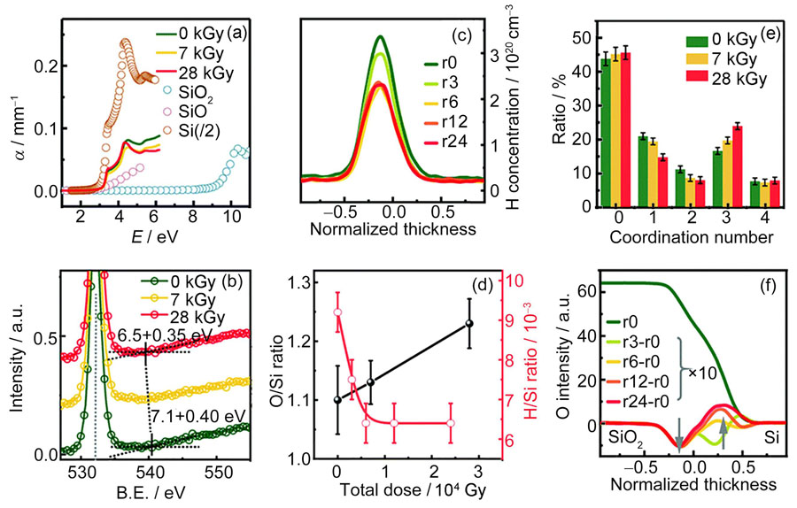
![TID-induced changes at the interface layer: (a) optical absorption spectra of the pristine and irradiated a-SiO2/Si interface, together with those of bulk SiO, Si and SiO2 for comparison; (b) the changes of band gaps of the ultra-thin films at different doses; (c) H distributions of samples irradiated at different doses obtained from sims (the r0, r3, r6, r12 and r24 labels mean that the films were irradiated to 0, 3, 6, 12 and 24 kGy; the original text using r0, r0.3, r0.6, r1.2, and r2.4 labels mean the films were irradiated to 0, 0.3, 0.6, 1.2 and 2.4 Mrad before sims measurements); (d) the O/Si ratios increase and H/Si ratios decrease with the increasing doses; (e) changes in the percentages of different chemical states of Si at different doses; (f) the distribution of O atom across the interface (green line), and gamma-ray irradiation-induced changes[5] (color online)](/richHtml/fsxb/2022/40/5/050101/img_01.jpg)
Fig. 1. TID-induced changes at the interface layer: (a) optical absorption spectra of the pristine and irradiated a-SiO2/Si interface, together with those of bulk SiO, Si and SiO2 for comparison; (b) the changes of band gaps of the ultra-thin films at different doses; (c) H distributions of samples irradiated at different doses obtained from sims (the r0, r3, r6, r12 and r24 labels mean that the films were irradiated to 0, 3, 6, 12 and 24 kGy; the original text using r0, r0.3, r0.6, r1.2, and r2.4 labels mean the films were irradiated to 0, 0.3, 0.6, 1.2 and 2.4 Mrad before sims measurements); (d) the O/Si ratios increase and H/Si ratios decrease with the increasing doses; (e) changes in the percentages of different chemical states of Si at different doses; (f) the distribution of O atom across the interface (green line), and gamma-ray irradiation-induced changes[5] (color online)
![(a) Annealing of defects induced by radiation of Ar ions: ○/● stands for the number of C atoms with one coordination before/after annealing; □/■ stands for the number of two-coordinated atoms before/after annealing; △ correspond to the number of sputtered C atoms; (b, c) schematic illustration of defects before and after annealing[20]](/richHtml/fsxb/2022/40/5/050101/img_02.jpg)
Fig. 2. (a) Annealing of defects induced by radiation of Ar ions: ○/● stands for the number of C atoms with one coordination before/after annealing; □/■ stands for the number of two-coordinated atoms before/after annealing; △ correspond to the number of sputtered C atoms; (b, c) schematic illustration of defects before and after annealing[20]
Fig. 3. N atom doping in graphene by co-irradiation with precursors[32]
Fig. 4. Vacancy defects in h-BN[43]
Fig. 5. Defects and adsorption performance of zeolite prepared by radiation[54]

Set citation alerts for the article
Please enter your email address


